
Ziyad Ahmed Al Tarawneh
Department of Electrical Engineering, Mu`tah University, Mu`tah, Karak, Jordan
Information Technology Journal
Year: 2016 | Volume: 15 | Issue: 3 | Page No.: 52-60


ABSTRACT
In this study, a novel approach in the design of a sub-picosecond time-to-voltage converter (TVC) based on the phenomenon of metastability in a bi-stable element is presented. The proposed TVC is a modified form of a TDC such that the timing information is transformed to a voltage directly without digitization. The measurement circuit is compact enough to be implemented on the chip. This, in turn, reduces the possibility of environmental noise interference. A detailed description of the time voltage conversion property is discussed. Simulations suggest that the time voltage converter can be designed for converting large gains with short input dynamic ranges which could be very useful in jitter measurement, especially in modern aggressive design styles where the resolution requirements on such measurements is in the picosecond range. Moreover, some figures of merit and performance parameters are introduced along with a discussion on some of the trade-offs involved in the design of the proposed TVC.
PDF Abstract XML References Citation
Received: April 16, 2016;
Accepted: May 10, 2016;
Published: June 15, 2016
How to cite this article
Ziyad Ahmed Al Tarawneh, 2016. Metastability Dependent Sub-picosecond Time-to-voltage Converter. Information Technology Journal, 15: 52-60.
DOI: 10.3923/itj.2016.52.60
URL: https://scialert.net/abstract/?doi=itj.2016.52.60
DOI: 10.3923/itj.2016.52.60
URL: https://scialert.net/abstract/?doi=itj.2016.52.60
INTRODUCTION
With rapid scaling and development in CMOS technology striving towards an increase in speed, higher performance and greater miniaturisation, even low levels of noise and signal interference such as cross talk, switching noise and substrate coupling become significant detrimental factors in signal integrity and have a severe impact on performance, consequently requiring the need for sophisticated signal processing techniques.
Time-to-digital converters (TDCs) present numerous advantages over conventional analog-to-digital converters (ADC’s). The TDCs can offer greater immunity to noise and interference, wider dynamic range, process scalability as well as simplicity in design and integration1. Some important applications of TDCs are in time-of-flight (TOF) laser radars for distance and velocity measurements2, RF synthesisers3, calibration of automatic test equipment systems4, telecommunication applications such as PM and FM demodulators and a broad spectrum of emerging applications such as digital storage oscillators5. Nonetheless, quite a number of applications are more challenging than others, consequently demanding uncompromising requirements on TDC designs. For example, on-chip jitter and delay measurement of a circuit requires ingenuity to obtain high resolution and precision of the timing quantities to be measured on-chip6-8.
Possibly the oldest and simplest TDC design is the single counter TDC implementation. This converter operates by counting the total number of clock cycles allocated in the time interval set between the START and STOP signals. This method is most often utilised as a supplementary block to higher resolution TDC systems to allow coarse measurements and expand the input dynamic range. An additional simple TDC design is the cyclic pulse-shrinking TDC. This type of converter measures the width of an incoming pulse by making use of a pulse-shrinking element. A simple example of this is the chain of inverters suggested in Tisa et al.9.
One particular problem with this type of design is the associated long measurement dead time, considering that the measurement of the incoming pulse width is directly dependent on the number of cycles in the loop. Even though this implies an almost unlimited input dynamic range, dead times could become progressively more notable for larger inputs rendering this architecture impractical for repeated measurements. Another challenge with this TDC is its sensitivity to temperature, w hich can influence both the carrier mobility and threshold voltage of a MOS transistor, requiring the need for a careful calibration procedure10.
In contrast to pulse-shrinking, the pulse-stretching technique digitises an incoming pulse by stretching the pulse to a more detectable level and using a measurement clock to count11. The stretch factor is implemented as the product of the current ratio and capacitor ratio in order to reduce the effect of process variability. In addition, analogous to flash ADCs, flash TDCs operate by comparing a signal edge to various reference signal edges displaced in time. However, in the case of the flash ADC, voltage comparisons are made by a comparator, its equivalent in the time-domain is the arbiter, which selects, which of the two input signals arrived first12,13. Despite the fact that the flash TDC can be utilised for medium resolution applications, this type of converter is not always useful for on-chip jitter measurement applications where results are often at sub-gate resolutions. Moreover, multiple vernier delay lines can overcome the limitation in temporal resolution of the flash7,14. Similar to the flash TDC, the output is thermometer coded and the input time difference is defined in Eq. 1, where, N represents the location of the first latched arbiter.
| (1) |
The effective time resolution accomplished within a VDL-based TDC is based on the matching between the various buffer cells. Having said that, in order to have a larger input range, a large number of VDLs needs to be used, which eventually leads to mismatching issues. Even with careful layout approaches, the mismatches cannot be completely eliminated.
The TDC architecture based on the time amplifier (TAMP) block described in Oulmane and Roberts15 and Siliang et al.16 can overcome many of the shortcomings found in past traditional TDC techniques. The time amplifier operates by enlarging small input time differences set by two time events, usually in the form of two rising edge signals. This amplification process helps alleviate some of the input range problems found in most high-resolution TDC designs. An elementary drawback of the TAMP TDC is the relatively long conversion time from input to output. In contrast to conventional voltage amplifiers, the TAMP must generate the amplified time information and consequently consuming time. Hence, the processing time is of the order of the output phase difference ΔΦout, excluding additional processing from the LR-TDC.
Time-to-voltage conversion is yet another analogue method frequently used, also referred to as the interpolation-based time-to-digital converter (TDC). It provides a substitute for the analogue-based interpolation schemes in that it is similar to the time stretching technique, though in this method the value of the voltage across the capacitor is directly read by an analogue-to-digital converter (ADC). Figure 1 shows a simplified circuit of the conversion of the time to voltage accompanied by the analogue-to-digital conversion stage.
In this technique, a constant current source is used to linearly charge a capacitor in order to convert the time interval (ΔT) into a voltage and then the voltage is held briefly to allow the analogue-to-digital (A/D) conversion. After the measurement, the capacitor is quickly discharged in an effort to minimise the dead time between different measurements. This method has been applied in many designs using discrete and Integrated Circuits (ICs)2,6,17. As the time-stretcher method, the time-to-voltage conversion can reach picosecond resolution. However, the constraint of this method is the limited dynamic measurement range which is determined by the maximum voltage to which the capacitor can be charged (i.e., the supply voltage). There are a number of ways to implement time to-analogue voltage converters (time interval measurements). Figure 2 demonstrates a preferred architecture of TVC, which consists of three building blocks. Firstly, a digital circuit is used to transform the two input signals into two complementary control pulses with time interval (ΔT). The corresponding quantity of charge that is integrated onto capacitor C is then determined by the analogue circuit which uses digital signals. Finally, the output voltage is captured by an ADC and transformed into digital form An and Roberts18.
Time-to-voltage converters can be easily constructed with discrete components and many IC designs while continue to deliver a time precision of 10 psec2 or even close to 1 psec19. Many IC designs are precise to around 20-40 psec11,20. Time-to voltage converters are widely used in various other applications other than TDCs21. For instance, in Taillefer and Roberts22, a delta-sigma ADC is designed using the voltage-to-time conversion methods, in which the integrator’s current is modified by the input voltage. Park and Perrott23 utilises a voltage-to-time converter and a gated ring oscillator (GRO)-TDC for A/D conversion.
In the following sections, the proposed TVC-based TDC architecture is presented. Furthermore, the TVC transfer curve behaviours are examined via parameter sweep simulations.
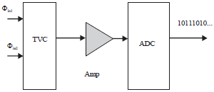 | |
| Fig. 1: | Time-to-voltage converter based TDC architecture |
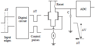 | |
| Fig. 2: | Basic building blocks of TVC18 |
In this study, measuring a very fine time difference is the main focus of the proposed TVC design. For instance, measuring the jitter of a recovered clock form a signal of a serial link.
DESIGN OF TIME TO VOLTAGE CONVERTER
The key idea of the proposed circuit is based on transforming distributions of time to distributions of voltage (TVC) utilising the phenomenon of metastability in digital circuits. In this study, a simple D-latch at metastable conditions is used to provide a metastable output which can be then used to control the charging path of the output capacitor as a result the voltage across the capacitor being proportional to the time interval of the input signals. Figure 3 shows the schematic diagram of the proposed time to voltage converter circuit. The proposed TVC circuit is compact enough to be implemented on a chip as it consists of ten MOS transistors and one minor load capacitor. The operation is accomplished in two stages. Firstly, a metastable state is generated at the output of D-latch which is initiated by the START event (CLK) which represents a rising edge and is terminated by the STOP event (data) which is represented by a falling edge. Secondly, the output voltage of D-latch after resolution of any metastability is then used to control the constant current source (PMOS) which charges up the output capacitor.
In other words, the output capacitor is charged up by a variable current source controlled by the metastable voltage at the output. The total charge delivered to the capacitor is then an analogue representation of the time interval to be measured. An analog-to-digital conversion can be then performed. To verify the time-to-voltage conversion ability of the proposed circuit described previously, simulations were performed using HSPICE circuit simulator and a 45 nm model card, with a single supply voltage Vdd = 0.9 V. The value of time offset at the input ΔФin =Фin1-Фin2, required to cause metastable events at the output of D-latch was varied at a time interval of 0.01 psec to generate the corresponding output metastable voltage in order to obtain precise results in the metastable region. Figure 4 shows the different TVC transient curves of Vout for different time intervals ΔФin ranging from -200 to 200 psec. As ΔΦin is increased, Vout experiences a monotonic increase while still maintaining its linear behaviour.
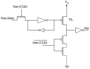 | |
| Fig. 3: | Circuit diagram of time-to-voltage converter |
Therefore, the relationship between ΔΦin and Vout can be used to move from a time–domain input to a voltage-domain output. By simply measuring the voltage at Vout at a given instant, the proposed circuit can now function closer to a TVC. Converting the circuit into a TVC has the added advantage of a quick data conversion time since voltage can be measured instantaneously as opposed to time. The input and output relationship of the TVC is defined as follows:
| (2) |
| (3) |
Note that in a TVC, input to output conversion occurs from the time-domain to the voltage-domain and will be represented by the TVC gain-conversion factor denoted as γ.
RESULTS AND DISCUSSION
In this section, circuit simulations were undertaken to demonstrate the effects of key design parameters such as capacitor configuration and transistor width on time to voltage conversion-gain and dynamic input range, where the dynamic range is defined as the difference between the maximum and minimum values of the time intervals that can be measured.
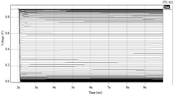 | |
| Fig. 4: | TVC transient curves of Vout for different time intervals |
 | |
| Fig. 5: | Influence of Vdd on time to voltage transfer characteristics |
 | |
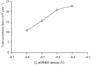
| Fig. 6: | Influence of Vdd on gain coefficient of time to voltage converter |
 | |
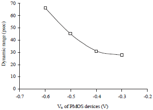
| Fig. 7: | Influence of Vdd on dynamic input range of time to voltage converter |
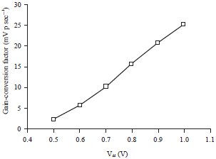
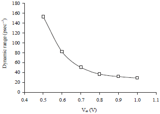
Defining the dynamic range also depends on the application’s requirements. Figure 5 illustrates the influence of supply voltage (Vdd) on the time to voltage transfer characteristics. Clearly as the supply voltage Vdd of the circuit decreases, the dynamic range of time to voltage conversing increases while the slope or gain of time to voltage decreases as demonstrated in Fig. 6 and 7.
This can be explained by approximating the average charging current of the controlled PMOS transistor (MP1) by the equation:
| (4) |
where, CL is the output capacitance, Vout is the output voltage, Vthp is the threshold voltage of the PMOS device (MP1) and KP is the transconductance parameter for the device, which is defined as:
| (5) |
The gate to source voltage Vgs of the PMOS device (MP1) can be represented as the difference between Vdd and the control voltage which is the voltage of the metastable output of a bi-stable circuit which exhibits metastability, given by:
| (6) |
The value of Vm is given by:
| (3) |
 | |
| Fig. 8: | Influence of CL on gain coefficient of time to voltage converter |
 | |
| Fig. 9: | Influence of CL on dynamic input of time to voltage converter |
where, θ is a circuit constant which determines the rate at which the overlap time between the data and clock is converted into a voltage difference between the two nodes of the cross-coupled inverters. The ΔTin is the time difference between the input signal and reference and τ is the metastability time constant of the bi stable element24, which is given as:
| (8) |
where, K is the ratio of the output capacitance to input capacitance, Cox is the gate capacitance per unit area, L is the device length and Wn and Wp are the channel widths for the n and p channel devices, respectively. The μn and μp are the mobility of holes and electrons, respectively and the magnitude of the threshold voltage, Vth, is equal for both p-channel and n-channel devices.
Substituting Eq. 6 into Eq. 4 yields:
| (9) |
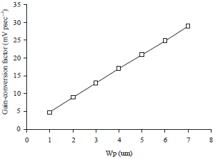 | |
| Fig. 10: | Influence of Wp on gain coefficient of time to voltage converter |
Finally, by solving the delay and differentiating with respect to Tin, the gain coefficient of time to voltage converter (γ) can be defined as:
| (10) |
where, toutm is the resolution time of a metastable event of the D-latch and tout is the delay time required to charge up the output capacitor. As evident from Fig. 5, 6 and Eq. 10, one can see that increasing the supply Vdd directly increases the gain coefficient of time to voltage converter, despite the fact that the Vdd is inversely proportional to the metastability time constant which means an increase in the ac gain of the inverter (by increasing gm).
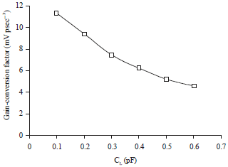
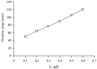
In a similar manner, it was noticed that increasing the load capacitance significantly increases the dynamic range while reducing the gain of time to voltage conversion as shown in Fig. 8 and 9.
Moreover, Fig. 10 and 11 show a plot of the effects of transistor width Wp1 on the TVC output signal. The result of larger transistor sizes on the TVC performance is a higher gain-conversion factor. Because of the inverse relation between transistor size and resistance, larger sizes result in smaller resistances, which reduce the average time constant of the system.
Figure 12 and 13 show the effect of threshold voltage NMOS devices. Clearly as the Vthn of the NMOS devices increases, the dynamic range and the gain of time to voltage conversion slightly increase.
Figure 14 and 15 demonstrate the effect of threshold voltage PMOS devices. Clearly as the Vthp of the circuit increases, the dynamic range of time to voltage conversion increases while the slope or gain conversion factor decreases. In summary, by carefully choosing the values of the capacitor CL as well as proper transistor sizing, the overall gain of the TVC can be manipulated.
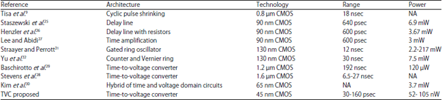
Table 1 presents performance summary and comparison of recent integrated TDCs that are suitable for applications in which a short measurement range is required.
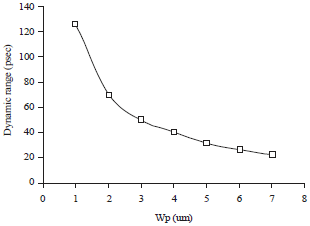 | |
| Fig. 11: | Influence of Wp on dynamic input of time to voltage converter |
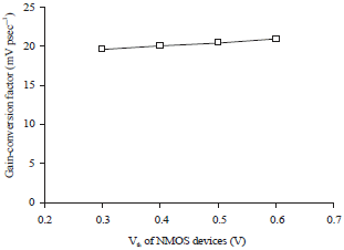 | |
| Fig. 12: | Influence of Vthn on gain coefficient of time to voltage converter |
In cyclic pulse-shrinking technique, for example, a single shrinking element in the delay line is utilised to effectively circulate the pulse in the actual delay line until eventually it vanishes. Thereafter, A counter counts the rounds of circulation and indicates the result. A dynamic range of 18 nsec was achieved with 20 psec resolution9.
In frequency synthesis, a TDC based on a delay line with successive elements are employed to digitize the cycle time of a GHz-level output signal or alternatively its phase difference with respect to a reference signal.
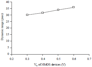 | |
| Fig. 13: | Influence of Vthn on dynamic input of time to voltage converter |
 | |
| Fig. 14: | Influence of Vthp on gain coefficient of time to voltage converter |
| Table 1: | Integrated TDCs with a short measurement range |
 | |
 | |
| Fig. 15: | Influence of Vthp on dynamic input of time to voltage converter |
The successive delay line measurement technique provides inverter delays of about 20 psec in 90 nm CMOS technology and can cover a 640 psec measurement range25. This gate delay was divided by using passive resistors between the delay elements so that 4.7 psec resolution and 3.3 psec precision could be attained in 90 nm CMOS when measuring over a 600 psec range26.
Another sub-gate delay measurement technique27 amplifies the residue between the timing signal and delay line and could achieve almost 1 psec measurement precision by means of complicated linearization methods and look-up tables.
More related study to TDC based on time to voltage conversion were presented by Stevens et al.28 and Baschirotto et al.29, nevertheless they unable provide such a short measurement range while consuming much higher power.
More recently, a TDC based on a hybrid of time and voltage-domain circuits is introduced by Kim et al.30. The TDC operates in two steps, i.e., first in the time domain by using a delay-line TDC and then in the voltage domain by utilising a successive-approximation-register analog-to-digital converter. The time residue of the first stage is converted to voltage by using a switch-based time-to-voltage converter (TVC) with the help of pseudo differential time-domain signalling. In the 65 nm CMOS technology, this study achieves 630 fsec of time resolution while consuming 3.7 mW from a 1.2 V supply.
In this study, it was found that the dynamic measurement range of the TVC proposed is in the order of 160 psec and it also could provides a resolution time in sub picoseconds. While consuming much lower power. However, The simpler element structure makes for better resolution but it also means that the resolution varies with temperature or operating voltage and from one circuit to another. A double ended VTC where the output can be measured differentially can overcome the vulnerability to PVT variations and noise effects in such single-ended TVC design.
CONCLUSION
A new design of very fine TVC based on the phenomenon of metastability in a bi stable element is presented, the TVC transfer curves were examined via parameter sweep simulations. The simulations were included to demonstrate the effects of key design parameters such as load capacitance and transistor width on time conversion-gain and dynamic input range. The gain can be increased or decreased by properly setting the width of the transistors in the proposed circuit. In future, a double ended VTC where the output can be measured differentially will be examined. This will be done in order to overcome the common problem in such single-ended TVC design of vulnerability to PVT variations and noise effects.
REFERENCES
- Yurish, S.Y., 2004. Sensors and transducers: Frequency output versus voltage output. Sensors Trans. Mag., 49: 302-305.
Direct Link - Maatta, K. and J. Kostamovaara, 1998. A high-precision time-to-digital converter for pulsed time-of-flight laser radar applications. IEEE Trans. Instrum. Meas., 47: 521-536.
CrossRefDirect Link - Ramakrishnan, V. and P.T. Balsara, 2006. A wide-range, high-resolution, compact, CMOS time to digital converter. Proceedings of the 19th International Conference on VLSI Design held jointly with 5th International Conference on Embedded Systems Design, January 3-7, 2006, Washington, DC, USA., pp: 197-202.
CrossRefDirect Link - Mantyniemi, A., T. Rahkonen and J. Kostamovaara, 2002. An integrated 9-channel time digitizer with 30 ps resolution. Proceedings of the IEEE International Solid-State Circuits Conference, Volume 1, February 7, 2002, San Francisco, CA, USA., pp: 266-465.
CrossRef - Rahkonen, T., E. Malo and J. Kostamovaara, 1996. A 3 V fully integrated digital FM demodulator based on a CMOS pulse-shrinking delay line. Proceedings of the IEEE International Symposium on Circuits and Systems, Volume 2, May 12-15, 1996, Atlanta, GA., pp: 572-575.
CrossRef - Tian, X. and J.C. Lo, 2003. Time-to-voltage converter for on-chip jitter measurement. IEEE Trans. Instrum. Meas. Soc., 52: 1738-1748.
CrossRefDirect Link - Chan, A.H. and G.W. Roberts, 2004. A jitter characterization system using a component-invariant Vernier delay line. IEEE Trans. Very Large Scale Integr. (VLSI) Syst., 12: 79-95.
CrossRefDirect Link - Chung, C.C. and W.J. Chu, 2011. An all-digital on-chip jitter measurement circuit in 65nm CMOS technology. Proceedings of the International Symposium on VLSI Design, Automation and Test, April 25-28, 2011, Hsinchu, pp: 1-4.
CrossRef - Tisa, S., A. Lotito, A. Giudice and F. Zappa, 2003. Monolithic time-to-digital converter with 20ps resolution. Proceedings of the 29th European Solid-State Circuits Conference, September 16-18, 2003, Estoril, Portugal, pp: 465-468.
CrossRefDirect Link - Chen, C.C., P. Chen, C.S. Hwang and W. Chang, 2005. A precise cyclic CMOS time-to-digital converter with low thermal sensitivity. IEEE Trans. Nuclear Sci., 52: 834-838.
CrossRefDirect Link - Raisanen-Ruotsalainen, E., T. Rahkonen and J. Kostamovaara, 2000. An integrated time-to-digital converter with 30-ps single-shot precision. IEEE J. Solid-State Circuits, 35: 1507-1510.
CrossRefDirect Link - Dudek, P., S. Szczepanski and J.V. Hatfield, 2000. A high-resolution CMOS time-to-digital converter utilizing a Vernier delay line. IEEE J. Solid-State Circ., 35: 240-247.
CrossRefDirect Link - Zhang, X.J., K.J. Cui, Z. Zou and L.R. Zheng, 2015. A low-power coarse-fine time-to-digital converter in 65nm CMOS. Proceedings of the International Symposium on Signals, Circuits and Systems, July 9-10, 2015, Lasi, pp: 1-4.
CrossRefDirect Link - Chen, P., C.C. Chen, J.C. Zheng and Y.S. Shen, 2007. A PVT insensitive vernier-based time-to-digital converter with extended input range and high accuracy. IEEE Trans. Nuclear Sci., 54: 294-302.
CrossRefDirect Link - Siliang, H., W. Donghui and L. Yan, 2013. A CMOS synchronous time amplifier. Proceedings of the IEEE 10th International Conference on ASIC (ASICON), October 28-31, 2013, Shenzhen, pp: 1-4.
CrossRefDirect Link - Collins, M., B.M. Al-Hashimi and N. Ross, 2005. A programmable time measurement architecture for embedded memory characterization. Proceedings of the European Test Symposium, May 22-25, 2005, UK., pp: 128-133.
CrossRef - An, D. and G.W. Roberts, 2008. A metastability-independent time-to-voltage converter. Proceedings of the IEEE International Symposium on Circuits and Systems, May 18-21, 2008, Seattle, WA., pp: 2298-2301.
CrossRef - Keranen, P., K. Maatta and J. Kostamovaara, 2011. Wide-range time-to-digital converter with 1-ps single-shot precision. IEEE Trans. Instrumentation Measur., 60: 3162-3172.
CrossRefDirect Link - Crotti, M., I. Rech and M. Ghioni, 2012. Four channel, 40 ps resolution, fully integrated time-to-amplitude converter for time-resolved photon counting. IEEE J. Solid-State Circ., 47: 699-708.
CrossRefDirect Link - Keranen, P. and J. Kostamovaara, 2013. Noise and nonlinearity limitations of time-to-voltage based time-to-digital converters. Proceedings of the IEEE Nordic-Mediterranean Workshop on Time-to-Digital Converters, October 3, 2013, Perugia, pp: 1-6.
CrossRef - Taillefer, C.S. and G.W. Roberts, 2009. Delta-sigma A/D conversion via time-mode signal processing. IEEE Trans. Circ. Syst. I: Regul. Pap., 56: 1908-1920.
CrossRefDirect Link - Park, M. and M.H. Perrott, 2009. A single-slope 80MS/s ADC using two-step time-to-digital conversion. Proceedings of the IEEE International Symposium on Circuits and Systems, May 24-27, 2009, Taipei, pp: 1125-1128.
CrossRef - Flannagan, S.T., 1985. Synchronization reliability in CMOS technology. IEEE J. Solid-State Circ., 20: 880-882.
CrossRefDirect Link - Staszewski, R.B., S. Vemulapalli, P. Vallur, J. Wallberg and P.T. Balsara, 2006. 1.3 v 20 ps time-to-digital converter for frequency synthesis in 90-nm CMOS. IEEE Trans. Circ. Syst. II: Express Briefs, 53: 220-224.
CrossRefDirect Link - Henzler, S., S. Koeppe, D. Lorenz, W. Kamp, R. Kuenemund and D. Schmitt-Landsiedel, 2008. A local passive time interpolation concept for variation-tolerant high-resolution time-to-digital conversion. IEEE J. Solid-State Circ., 43: 1666-1676.
CrossRefDirect Link - Lee, M. and A.A. Abidi, 2008. A 9 b, 1.25 ps resolution coarse-fine time-to-digital converter in 90 nm CMOS that amplifies a time residue. IEEE J. Solid-State Circ., 43: 769-777.
CrossRefDirect Link - Stevens, A.E., R.P.V. Berg, J.V.d. Spiegel and H.H. Williams, 1989. A sub-nanosecond time-to-voltage converter and analog memory. Proceedings of the IEEE International Symposium on Circuits and Systems, May 8-11, 1989, Portland, OR., pp: 268-271.
CrossRefDirect Link - Baschirotto, A., G. Boella, R. Castello, G. Frattini, G. Pessina and P.G. Rancoita, 1998. 3ns resolution CMOS low-power time-to-voltage converter. Electron. Lett., 34: 614-615.
Direct Link - Kim, J., Y.H. Kim, K.S. Kim, W. Yu and S.H. Cho, 2015. A hybrid-domain two-step time-to-digital converter using a switch-based time-to-voltage converter and SAR ADC. IEEE Trans. Circ. Syst. II: Exp. Briefs, 62: 631-635.
CrossRefDirect Link - Straayer, M.Z. and M.H. Perrott, 2008. An efficient high-resolution 11-bit noise-shaping multipath gated ring oscillator TDC. Proceedings of the IEEE Symposium on VLSI Circuits, June 18-20, 2008, Honolulu, HI., pp: 82-83.
CrossRefDirect Link - Yu, J., F.F. Dai and R.C. Jaeger, 2010. A 12-bit vernier ring time-to-digital converter in 0.13μm CMOS technology. IEEE J. Solid-State Circ., 45: 830-842.
CrossRefDirect Link