
Pooya Assadi
Islamic Azad University, Varamin-Pishva Branch, Iran
Journal of Applied Sciences
Year: 2008 | Volume: 8 | Issue: 14 | Page No.: 2625-2630


ABSTRACT
A new high-speed low-power multiplier has been presented in nanotechnology. Implementing multiplication algorithms in nanotechnology has a major effect in performance of arithmetic processors. A new design for the use of the number system {0, 1, 2, 3}, with a particular three bit coding of digits, is evaluated and some improvements are obtained, including the possibility of using a two bit coding, with a considerable reduction in the wiring of the multiplier structure. Non-regularities in the construction of conventional Wallace tree multipliers consequence in a large quantity of dissipated area when implemented in VLSI. A novel Wallace tree structure is proposed. An evaluation between the critical path and wiring overhead between the conventional and the modified Wallace tree is presented. A fast adder has been implemented. The proposed adder is based on carry chain schemes. A Wallace tree multiplier is designed and simulated in a 70 nm process. We used HSPICE and Synopsys for simulations. The latency has decreased by almost 18% and power consumption decreased by 16%. Our design reduced transistor count by 12%.
PDF Abstract XML References Citation
How to cite this article
Pooya Assadi, 2008. A Novel Multiplication Algorithm in Nanotechnology. Journal of Applied Sciences, 8: 2625-2630.
DOI: 10.3923/jas.2008.2625.2630
URL: https://scialert.net/abstract/?doi=jas.2008.2625.2630
DOI: 10.3923/jas.2008.2625.2630
URL: https://scialert.net/abstract/?doi=jas.2008.2625.2630
INTRODUCTION
Multiplication is one of the important arithmetic operations. In fact 10% of all instructions in a scientific program are multiplies (Van and Yang, 2005). In addition, multiplication is a long latency operation. In processors, multiplication takes between two and eight cycles. Therefore, having high-speed multipliers is important for the performance of processors. With the advent of nanotechnology, the requirements for low power, high-speed designs have become more important. In this study, we have decreased technology size from 130 to 70 nm. Decreasing technology size and transferring to nanotechnology changes our view of methods to design high-speed arithmetic operators. Using nanotechnology has major effect in power and delay. In response to the high request of fast computer graphics, floating-point computation, etc., multiplier components are included in nearly every digital signal processor as well as arithmetic processors. To achieve high speed, the Wallace tree structure and modified Booth recording technique is used because it uses the partial products in parallel in a tree structure. Because of its irregularity, the layout of Wallace tree multipliers has a large dissipated area (e.g., 25%) when laid out in a rectangular area which is the conventional form of layout when many different units are to be communicate with each other. Since cost is a third power function of area, when implementing high-speed multipliers in VLSI, a main part of area and time is used up on computing partial products using some kind of tree structures. Formerly, these were based on the use of full-adders (and rarely some half-adders), decreasing the sum of three rows of bits to the sum of two, using either the Wallace- or Dadda-architectures of the tree structure. As these architectures are not very regular to layout because of the three to two architecture, it was requested to use four to two adders which let the use of binary tree architectures. Van and Yang (2005) are the first to present their use, based on the carry-save demonstration, where two operand are computed and encoding of a single operand shows redundant number system {0, 1, 2}. Therefore the four to two adder can be computed and adder taking two such operands and adding them to generate the result in the same demonstration. This addition can be executed in parallel and therefore in regular time, using an array of such adders. Radix two signed-representation for four to two adders over the digit number system {-1, 0, 1} were then later proposed by Chong et al. (2007). Recently a new design has been proposed (Kumar et al., 2006) using the number system {0, 1, 2, 3} with a particular three bit coding of the digits and most recently novel designs (Sousa and Chaves, 2005) compared different three and four component number systems using some coding, considering major differences in the design of these. Other articles discussing multiplier architectures are presented (Kaihara and Takagi, 2008). Multipliers have an important effect on arithmetic processors performance. A new high-speed low-power multiplier has been presented in nanotechnology.
MATERIALS AND METHODS
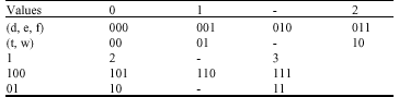
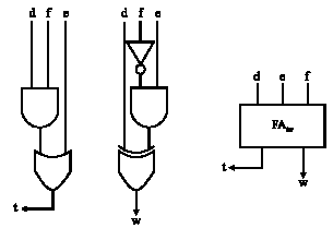
This study started in 2007 at Microelectronic Center of Islamic Azad University Varamin-Pishva Branch. An example using the number system {0, 1, 2, 3} was presented by Van and Yang (2005). This implementation was proposed using the number system {0, 1, 2, 3}, although with a three bit coding of digits, where the value of the expression can be computed by adding the values of the three bits (d, e, f) for all the valid combinations, v = d+e+f, where (e, f) ≠ (1, 0). Also, a two bit coding (t, w) was used. Three bit coding and two bit coding is shown in Table 1. Notice that (t, w) is the similar coding as in Chong et al. (2007) for the number systems D(CS 2) = {0, 1, 2} and D(CS 3) = {0, 1, 2, 3} with value d = 2dh + dl. Transferring from (d, e, f) into (t, w) is done by the logic in Fig. 1 (to some extent restructured from Sousa and Chaves (2005), here using exclusively AND, OR and XOR gates), shown together with a simplified structure of it.
This logic is practically like to a full-adder, except for the limitations on the input (d, e, f) (which we will indicate the encoding) and coding of the output in the (t, w)-shape. Kumar et al. (2006) then explains different adders for combinations of operands in the redundant coding. We will only go into particulars with two of these. The first we explain in Fig. 2 is an adder taking four normal binary operands and transferring their sum in the encoding, again somewhat improved from Kaihara and Takagi (2008).
Notice here that the most significant section of Fig. 2, calculating (tout, d), is a conventional full-adder and the least significant section is a encoding where e+f = i+t, but shows that only valid bits of d, e, f are generated ((e, f) ≠ (1, 0)). This is the structure required at the first level of a multiplier structure, the critical path here is two XOR gates and it results a speedup compared to a conventional four to two adder. For the case of two operands the critical path is two XORs, plus an AND and an OR gate, where it also resulted a speedup. The following diagram shows how the addition is done:
Any multiplier can be partitioned into three steps: Partial products generation step, partial products addition step and the final addition step.
| Table 1: | Three bit coding and two bit coding |
 | |
 | |
| Fig. 1: | Transferring from (d, e, f) into (t, w) |
 | |
| Fig. 2: | Adder using four binary inputs (d, e, f) |
In the first step, the multiplicand and the multiplier are multiplied bit by bit to produce the partial products. In this step, a modified Booth coding algorithm is used instead to decrease the number of partial products to half. The second step is very important, as it is the most complex and shows the speed of the whole multiplier. This part will be concentrated on the improvement of this step, which includes the addition of all the partial products. If speed is not an important parameter, the partial products can be added in sequence, decreasing the plan difficulty. But, in high-speed implementations, the Wallace structure is conventionally used to add the partial products in a tree architecture in order to generate two rows of partial products that can be added in the last step. Although high-speed, because its critical path delay is relative to the logarithm of the number of bits in the multiplier, the Wallace tree has other problems such as dissipated layout area and increased complexity, which we will evaluate on shortly.
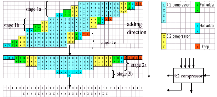 | |
| Fig. 3: | Conventional Wallace tree structure |
In the last step, the two-row outputs of the tree are added using any high-speed adder such as look-ahead adder to produce the output result.
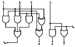
Wallace tree structure: There are a number of methods to design the Wallace tree. One way uses all the bits in each column and adds them into two bits (a sum and a carry). A second way, which is used in this paper, uses all the bits in each fours row and adds them in an appropriate method (Fig. 3). In Fig. 3, the Wallace tree uses four to two counters, three to two counters, full adders and half adders to add a 12 partial products tree. Each four to two counter takes in four bits from the same step j, one bit from the preceding step j-1 (which is the carry out of the counter in the preceding place) and outputs one sum bit in the place j and two carry outs into the next place j+1.
For final addition stage, a new adder has been proposed. As for any carry-skip adder, the worst propagation delay of the presented circuit can be partitioned into three steps: the carry produce delay, the carry-skip delay and the carry-attract delay (Van and Yang, 2005). In detail, a long carry chain begins at a general unit Bi, propagates through some bits in that unit (carry-produce), therefore skips some units (carry-skip) and split ends in a unit Bj (carry-attract). The common unit Bj is able to calculate its sum bits in parallel when its carry-in has to be internally chained through several bit places. Therefore, the delay due to the attraction of a transmitting carry from a previous unit is minimized.
Adder architecture: Figure 4 shows the Adder architecture of the new 64-bit adder. It uses non-regular linearly growing unit sizes, which appears as being 1, 3, 4, 5, 6, 7, 8, 9, 10 and 11 from the least significant bit to the most significant bit. This sizing measure allows the logic levels in the critical path to be minimized. Between two following units an inverting two to one multiplexer is used to do the omit action depending on the signal omit.
The signals section 0 and section 1 are used to organize slicing on the based of the required length (8-, 16-, 32-, or 64-bit). When slicing is not needed, the adder executes as a usual 64-bit carry-skip adder with low carry-attract delay. However, when additions on lower length have to be done the units in the adder must be properly sliced.
Since the lowest length operations need 8 bits, the less significant units never required to be sliced. On the other hand, significant units can be reorganized by means of section 0 and section 1 signals. There, expression (x-bit, y-bit) means that the (x+y)-bit unit is partitioned into two sub units of bits using one of the x more valued bits and the other of the y less valued bits. When slicing is needed section 0 and section 1 is used to determine that carry chain cannot result between these sub units. Because of that, parallel operations on multiple data are done and multiple independent results are produced. Thus, reorganizing a unit means slicing its carry-propagate in order to the appropriate bit place and ineffective the skip process between the current unit and the next unit. For example, for 8-bit slicing, the 6-bit unit carry-propagate has to be broken into the third-bit place, whereas the 5-bit unit carry-propagate has to be partitioned in the first-bit place, that is the unit does not get the carry chain coming form preceding units.
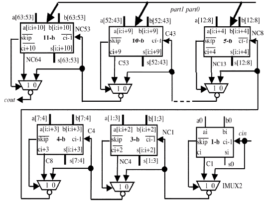 | |
| Fig. 4: | Adder architecture of the new 64-bit adder |
It is not important that units using an odd number of bit places, the one bit unit excepted, receive inverted carry in (NCi) and produce inverted carry out, whereas the other units get direct carry in (Cj) and generate direct carry out. This is because of using multiplexers in doing the skip process and in calculating the units of the adder. Multiplexers have been chosen to have non-inverting ones and to AND-OR architectures because of to minimize both delay and power. In detail, for the implementation technology, a minimum size multiplexer has a worst-case delay and a power consumption of 2.1 ns and 0.226 μW. Both parameters are lower than those shown by multiplexers and AND-OR architectures. The above case also shows a comparison with the adders presented in Kaihara and Takagi (2008).
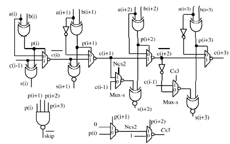
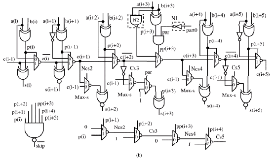
Units of bits: The new units have been designed without the addition of extra components or loads into the carry-chain path with respect to units. In Fig. 5a and b, the new 4-bit and 6-bit units are showed. The previous does not need reorganizing property while the latter does. Both the showed units contain an even number of bit places and they get positive carry in. Therefore, only inverting multiplexers are used in their carry-chains to form positive carries out. On the other hand, the units including odd number of bit places get negated carries in. Thus, at least one multiplexer has to be used in their carry-propagates to show negated carries out. We determined to use this multiplexer in the most significant bit place of the unit.
RESULTS AND DISCUSSION
A novel multiplier structure has been presented. For the final step of multiplication algorithm, a new 64-bit adder has been proposed. From Fig. 5 it can be seen that the multiplexers make the new unit able to minimize the carry-attract time. In detail, they allow the unit carry in c(i-1) to be straight use in sum bits calculation without waiting for its chain through the bit places into the unit itself. In order to obtain this, secondary signals Csk (with k odd) and NCsh (with h even) are calculated as the logic AND and the logic NAND, respectively, of the chain signals p(i), p(i+1), …, p(i+4). Consider that Csk and NCsh are obtained by using a multiplexer propagation. For the six bit unit, slicing is needed either for 8- or for 16-bit additions, that is, when section 0 = 1. Thus, in order to guarantee reorganization a simple inverter is used in the logic step to design the signal (i.e., to decode the slicing instructions). When signal is low the sum bit s(i+3) is calculated considering a low carry in and deleting both the unit carry in c(i-1) and the carry c(i+2) coming from the preceding bit places into the same unit.
| ||
 | ||
| Fig. 5: | Novel units (a) 4-bit and (b) 6-bit | |
In this case, no carry signal must be chained through the bit place i+3, thus signal do the signal pp(i+3) low state and the multiplexer calculating c(i+3) selects the inverted produce expression generated by the NAND gate. In parallel, because of pp(i+3) results low signals Ncs4 and Cs5 become high and low, respectively. Therefore, the submits s(i+4) and s(i+5) become free of c(i-1). Moreover, the signal will be high and then the skip process is done. It is easy to understand that when slicing is not required such unit works as a traditional carry-chain part inside a carry-skip adder with low carry-attract time (Sousa and Chaves, 2005). The carry chain path [i.e., from c(i-1) to c(i+5)] and the loads on its middle parts are both unaffected with respect to a unit without reorganizing property. Moreover, the secondary circuit used for slicing does not affect the length of the carry propagate. This is because of the fact that the right path for a carry chaining through a unit endowed with that secondary circuit is already recognized when the incoming carry receives.
It is not important that a 5-bit, 7-bit, 9-bit and 11-bit units have to be sliced only when eight bit additions have to be done. Therefore, a NAND gate is used in the logic step to code slicing instructions (i.e., to calculate ![]() ). in contrast, inside the 6-bit and 10-bit units, in which slicing is required either for 8- or for 16-bit additions, partition instructions are recognized by using a simple inverter producing
). in contrast, inside the 6-bit and 10-bit units, in which slicing is required either for 8- or for 16-bit additions, partition instructions are recognized by using a simple inverter producing ![]() . Finally, for the 8-bit unit a NOR gate is used to produce
. Finally, for the 8-bit unit a NOR gate is used to produce ![]() . This shows the constant necessity for the 8-bit unit slicing to be taken into account except when section 0 = section 1 = 0.
. This shows the constant necessity for the 8-bit unit slicing to be taken into account except when section 0 = section 1 = 0.
It can also easily examined that the longest carry-produce path of the general k-bit clock in the new adder has a delay equal to τXOR + 2τMUX, where τXOR and τMUX are the chain delays of a XOR gate and a two to one multiplexer, respectively. For example, the 6-bit unit in Fig. 5b shows a carry-produce delay of τXOR+6τMUX and a maximum carry-attract delay of τXOR+2τMUX due to the configuration of the submit s(i+3).
CONCLUSIONS
A new high-speed multiplier for nanotechnology based systems has been designed and simulated. Transferring to nanotechnology scale (e.g., 70 nm process as implemented here) has major effect in designing arithmetic operators. The new circuit has been verified using CMOS standard cells and then compared with previous designs. It has been shown that the new adder has the same speed as the circuit showed in Kaihara and Takagi (2008) with power and area about 13 and 18% reduction, respectively. A new design to use a radix two, four component number system with a three bit digit coding, has been analyzed. It was shown that this algorithm is only slightly different from the adder in Kumar et al. (2006) also using the number system {0, 1, 2, 3} and therefore can also be used as a common four to two, carry-save adder. It was furthermore represented that the three-bit coding is not essential and a standard two bit coding can be used, thus considerably decreasing the difficulty of the wiring of adder structure. In fact, the difference is only in the understanding of where the limitations between the steps in a multiplier structure are placed.
| Table 2: | Comparison between 32x32 bit multipliers |
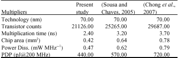 | |
| nm: Nanometer; ns: Nano second; MHz: Mega hertz | |
The dissipate area problem of big Wallace tree multipliers can be solved with a new way of tree structure. The improved tree has a smaller critical path but a larger wiring. Simulations have been done with HSPICE and Synopsys. Table 2 shows comparisons between multipliers. The latency has decreased by almost 18% and power consumption decreased by 16%. Our design reduced transistor count by 12%.
REFERENCES
- Chong, K.S., B.H. Gwee and J.S. Chang, 2007. Low energy 16-bit booth leapfrog array multiplier using dynamic adders. IET Circuits Devices Syst., 1: 170-174.
CrossRef - Kaihara, M.E. and N. Takagi, 2008. Bipartite modular multiplication method. IEEE Trans. Comput., 57: 157-164.
CrossRef - Kumar, S., T. Wollinger and C. Paar, 2006. Optimum digit serial GF(2^m) multipliers for curve-based cryptography. IEEE Trans. Comput., 55: 1306-1311.
CrossRef - Sousa, L. and R. Chaves, 2005. A universal architecture for designing efficient modulo 2 multipliers. IEEE Trans. Circuits Syst. I: Fundemental Theor. Applic., 52: 1166-1178.
CrossRef - Van, L.D. and C.C. Yang, 2005. Generalized low-error area-efficient fixed width multipliers. IEEE Trans. Circuits Syst. I: Fundemental Theor. Applic., 52: 1608-1619.
Direct Link