
Xiao Kui Li
China Coal Technology Engineering Group Chongqing Research Institute, Chongqing, 400700, China
Information Technology Journal
Year: 2014 | Volume: 13 | Issue: 14 | Page No.: 2318-2325


ABSTRACT
In this study, the application of ZCS synchronous rectification for the IPT resonant converter is researched. A novel control method that AC-DC section of the resonant converter works in ZCS SR state is proposed by using the characteristic of resonant tank current. First, the ZCS working operation of SR is presented, analyzed and equivalent circuits for each operation mode are also given, respectively. Then, the novel control method of ZCS SR for resonant converter is proposed. According to the ZCS working operation of SR and the differential equations of equivalent circuit, a steady-state mathematical model of the circuit is established. On that basis, the calculation method for ZCS operating point of SR is deduced by solving the fixed point function about resonant tank current. Moreover, the specific flow chart for calculating ZCS operating point of SR and the steady-state waveforms of each state variable is also presented and operating principle of control circuit for ZCS SR is described in detail. Finally, experimental results verify the effectiveness of control method proposed in this study.
PDF Abstract XML References Citation
Received: January 03, 2014;
Accepted: April 07, 2014;
Published: June 07, 2014
How to cite this article
Xiao Kui Li, 2014. Research ZCS Synchronous Rectification of Resonant Converter. Information Technology Journal, 13: 2318-2325.
DOI: 10.3923/itj.2014.2318.2325
URL: https://scialert.net/abstract/?doi=itj.2014.2318.2325
DOI: 10.3923/itj.2014.2318.2325
URL: https://scialert.net/abstract/?doi=itj.2014.2318.2325
INTRODUCTION
Because Synchronous Rectifier (SR) uses MOSFET switch owned very low on-resistance to replace the diode, it has been widely adopted in AC-DC converter. Therefore, SR has become a research hotspot in all kinds of switching power supply.
Analyzing the existing synchronous rectifier converters, such as buck converter (Yeh and Lai, 2012), push-pull converter, forward converter (Coban and Cadirci, 2011), half-bridge converter (Jeong, 2008), flyback converter (Kim et al., 2014), it can be found that their rectifier section generally work in hard switching state and switching losses for SR is inevitably generated. Further analysis shows that conventional switching power supply topologies are larger and less transmission efficiency when a larger power SR output.
Although many studies on SR already exists, but the application of ZCS SR in a resonant converter has been rarely studied. Therefore, the application of Zero Current Switching (ZCS) synchronous rectification for the Inductive Power Transfer (IPT) (Dai and Sun, 2014) resonant converter is researched. By using the characteristic of resonant tank current, a novel control method that AC-DC section of the resonant converter works in ZVS SR state is proposed.
ZCS OPERATION PRINCIPIE OF SR
In this study, the main circuit of IPT resonant converter used full-bridge synchronous rectifier, is shown in Fig. 1 which consists of a primary and a secondary circuit. In the primary circuit, voltage source Edc and inductance Ldc constitute a quasi current source. The two main IGBT switching pairs (S1, S4 and S2, S3) of the full-bridge inverter network alternate the direction of charging current into the resonant tank which consists of LP and CP. Therefore, a high-frequency Ac Can be generated in the primary coil LP. The coil LP as the transmitter transfers the high-frequency resonant energy to the pickup coil LS1 by the magnetic fields coupling. The inductor LS1 is completely tuned by the parallel capacitor CS and inductor LS2 and the AC voltage vSR is converted into a DC voltage by a full-bridge SR network constituting of the two MOSFET switching pairs (Q1, Q4 and Q2, Q3). The Co constitute a filter link, RL is the load resistance and M is the mutual inductance coupling between primary coil LP and secondary LS1 .
In order to simplify the following analysis, three assumptions are made for the analyses of operating modes:
| • | All IGBTs and MOSFETs are considered to be ideal |
| • | Input voltage source Edc is ideal |
| • | Filter capacitor Co is considered to be ideal |
Critical operation waveforms of the system are given in Fig. 2, for steady-state operation. The Iin is the input current of the primary parallel resonant tank consisting of LP and CP. As vCp is the voltage across capacitor CP. The vSR is the input AC voltage of full-bridge SR network. The iLs2 is the flowing current of inductor LS2. The vQi (i = 1, 2, 3, 4) is the drain-source voltage of switch Qi in the secondary SR network, respectively.
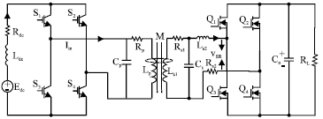 | |
| Fig. 1: | Main circuit of IPT resonant converter used full-bridge synchronous rectifier |
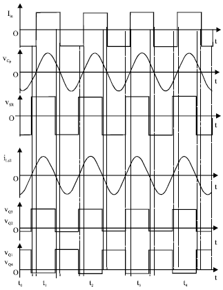 | |
| Fig. 2: | Critical steady-state operation waveforms |
Meanwhile, so as to clearly analyze operation modes of the main circuit shown in Fig. 1, time t0 is assumed to be the starting point of one operational cycle. In the primary circuit, shown in Fig. 1, stipulate positive direction of the quasi current s ource injected is that switches S1 and S4 are turned on when switches S2 and S3 are turned off. In the secondary circuit, shown in Fig. 1 , SR output positive direction of the AC voltage vSR is that when switches Q1 and Q4 are turned on and Q2 and Q3 are turned off. So, according to Fig. 2 and the foregoing assumptions, effective circuits for each mode in one operational cycle can be obtained in Fig. 3.
Mode 1 (t0-t1): The state of primary circuit is that quasi current source Iin energy is injected from negative direction and AC voltage vCp is less than zero. The IGBT switches S2 and S3 are turned on when S1 and S4 are turned off. The state of secondary circuit is that the AC voltage vSR is output from positive direction of the synchronous rectifier and current iLs2 is greater than zero. MOSFET switches Q1 and Q4 are reversely turned on when Q2 and Q3 are turned off. In this mode, its equivalent circuit is shown in Fig. 3a.
Mode 2 (t1-t2): The state of primary circuit is that quasi current source Iin energy is injected from positive direction and AC voltage vCp is greater than zero. The IGBT switches S1 and S4 are turned on when S2 and S3 are turned off. The state of secondary circuit is that the AC voltage vSR is output from positive direction of the synchronous rectifier and current iLs2 is greater than zero. MOSFET switches Q1 and Q4 are reversely turned on when Q2 and Q3 are turned off. In this mode, its equivalent circuit is shown in Fig. 3b.
Mode 3 (t2-t3): The state of primary circuit is that quasi current source Iin energy injected from positive direction and AC voltage vCp is is greater than zero. The IGBT switches S1 and S4 are turned on when S2 and S3 are turned off. The state of secondary circuit is that the AC voltage vSR is output from negative direction of the synchronous rectifier and current iLs2 is less than zero. MOSFET switches Q2 and Q3 are reversely turned on when Q1 and Q4 are turned off. In this mode, its equivalent circuit is shown in Fig. 3c.
Mode 4 (t3-t4): The state of primary circuit is that quasi current source Iin energy is injected from negative direction and AC voltage vCp is less than zero. IGBT switches S2 and S3 are turned on when S1 and S4 are turned off. The state of secondary circuit is that the AC voltage vSR is output from negative direction of the synchronous rectifier and current iLs2 is less than zero. MOSFET switches Q2 and Q3 are reversely turned on when Q1 and Q4 are turned off. In this mode, its equivalent circuit is shown in Fig. 3d.
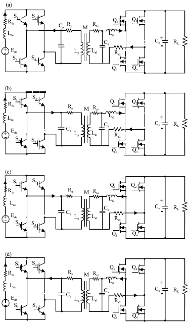 | |
| Fig. 3(a-d): | Equivalent circuits for each operation mode, (a) Mode 1, (b) Mode 2, (c) Mode 3 and (d) Mode 4 |
Through the above analysis, the IGBTs switching states of two primary switching pairs (S1, S4 and S2, S3) are changed, when the voltage vCp across capacitor is equal to zero. It means that their switching states are changed between turned on and off, the drain to source voltage of the four switches (S1, S4 and S2, S3) are also equal to zero. Therefore, the primary switching inverter works in zero voltage soft switching state.
In the secondary circuit, the current iLs2 flowing the inductor LS2 is a sinusoidal current. It is clear to know that when iLs is equal to zero, the current flowing the four MOSFET switches (Q1, Q2, Q3 and Q4) are also equal to zero. Therefore, ZCS SR output of the AC voltage vCp can be achieved by controlling the switching pairs (Q1, Q4 and Q2, Q3) turned on or off when iLs2 is equal to zero.
In summary, the primary full-bridge converter working in zero voltage soft switching state and the secondary full-bridge SR network working in zero current soft switching state can be achieved in the IPT resonant converter as shown in Fig. 1.
STEADY STATE MODELING OF CIRCUIT
In order to carry out the numerical analysis of the circuit as shown in Fig. 1, a steady-state mathematical model of the system is necessary to be established.
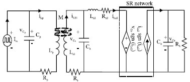 | |
| Fig. 4: | Equivalent circuit of the IPT resonant converter used ZCS SR |
Assume that the switching period of the primary full-bridge inverter (Fig. 1) is T under steady-state conditions. Then the input quasi current source Iin of the primary resonant tank can be described as presented in Eq. 1 and 2:
| (1) |
| (2) |
where, m is zero or a positive integer.
According to the ZCS operation principle of SR for the IPT resonant converter, switches transitions of the full-bridge SR network in the secondary are determined by the polarity change of the resonant current iLs flowing the inductor LS2. Consequently, define a sign function to represent operation of the full-bridge SR network (Eq. 3):
| (3) |
After such representations, the circuit diagram (Fig. 1) is simplified as an equivalent circuit (Fig. 4).
According to Kirchhoff=s current and voltage laws, the differential equations of the equivalent circuit as shown in Fig. 4, can be presented as follows:
| (4) |
| (5) |
| (6) |
| (7) |
| (8) |
| (9) |
| (10) |
Where:
Δ = LS LP-M2
Let:
x = [idc vCp iLp iLs1 vCs iLs2 vCo]T
and u = [Edc] be the state vector and the input vector of the system, respectively. According to the differential equations Eq. 4-10, the complete state space model in one cycle can be expressed as:
| (11) |
where, i represent the figures of operation modes in Fig. 3 and:
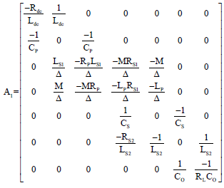  |
DETERMING ZCS-OPERATING CYCLE OF SR
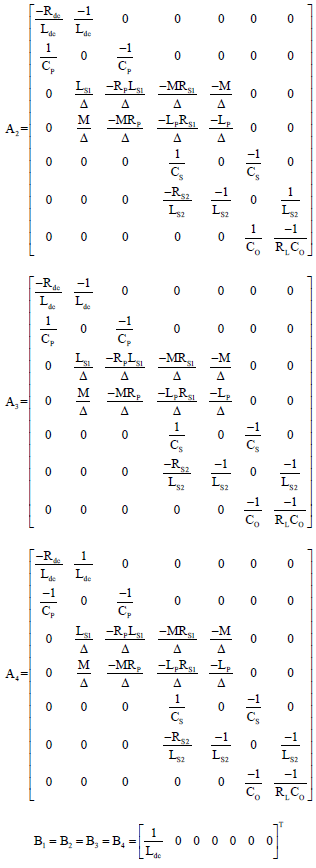
The ZCS operating point of the SR circuit must be obtained to make full-bridge SR network of the secondary circuit work in zero current soft switching state.
Because the system matrix A1, A2, A3, A4 are invertible, so, the analytical solution of Eq. 11 can be written in the following format (Eq. 12):
| (12) |
Where:
x0 = x(t)|t = 0
φ (t) = eAt x(t)
As it can be seen from Fig. 2 and 3, once the system is operating in steady state, its states repeat periodically. During one operational cycle, the final value of each mode equals to the initial value of the next mode. Therefore, Eq. 12 can be extended into four stroboscopic mapping equations (Eq. 13-16) to cover all the four modes (Liu et al., 2011):
| (13) |
| (14) |
| (15) |
| (16) |
where, ![]() , (i = 1, 2, 3, 4), I is a 7-order unit matrix and x0 is the initial value of the circuit state vector.
, (i = 1, 2, 3, 4), I is a 7-order unit matrix and x0 is the initial value of the circuit state vector.
When the system is in steady-state operation, the state vector repeats periodically. So, a fixed point x* about the state vector can be described in Eq. 17:
| (17) |
Substitute Eq. 14-16 into Eq.13, the fixed point x* can be specifically described as in Eq. 18:
| (18) |
Where:
α = (I-φ4φ3φ2φ1)-1
Corresponding to the ZCS condition of the full-bridge SR network, the switching states of four MOSFET switches (Q1, Q2, Q3 and Q4) are changed when iLs2 is equal to zero.
 | |
| Fig. 5: | Flow chart for calculating, TZCS and steady state warefarms |
Then from Eq. 17, ZCS operation cycle TZCS of the full-bridge SR network can be obtained as follows (Tang et al., 2009; Sun et al., 2011):
| (19) |
where, Y = [0 0 0 0 0 1 0] is a selection matrix for the state variable iLs2.
Once TZCS is obtained by solving the Eq. 19, let x* be the initial state vector x0. Then, calculate the analytical function Eq. 13-16 mode-by-mode. The steady-state waveforms of each state variable can be easily obtained. The specific flow chart for calculating TZCS and the steady-state waveforms of each state variable is shown in Fig. 5.
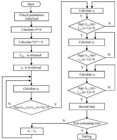
ZCS SR OPERATING PRINCIPIE OF CONTROL CIRCUIT
In order to achieve zero current soft switching state operation of the secondary full-bridge SR network, the ZCS SR working operation of control circuit as shown in Fig. 6.
The operational processes of the control circuit are described as follows. First, Current sensor converts the current iLs2 sampling signal to a voltage signal vs. The phase of the signal vs must be compensated, because the control circuit operation can lead to a delay of the signal. According to the above analysis, the zero time of current iLs2 is critical. When design the circuit to precisely control MOSFET switching pairs (Q1, Q4 and Q2, Q3) turned on or off, the zero-crossing detection circuit of current iLs2 consists of high-speed comparator LM311. Then, after the previous circuit, the digital signal Gi2 can be obtained. The G i2 is used as the input of bootstrap driver circuit for MOSFET switches (Q2, Q4). In order to achieve the two SR switching pairs (Q1, Q4 and Q2, Q3) working in zero current soft switching state, the two drive voltage pairs (Ugs1, Ugs4 and Ugs2, Ugs3) must be complementary. So, invert Gi2 and then Gi1 is used as the input of bootstrap driver circuit for switches (Q1, Q3). The control circuit for ZCS SR operation needs 5 and 15 V power supply. Because bootstrap driver circuit is used, 5 and 15 V power input is from the output voltage vCo.
 | |
| Fig. 6: | Control circut of the full-bridge ZCS SR |
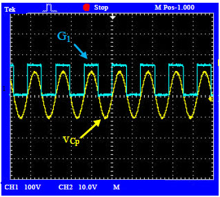 | |
| Fig. 7: | Experimental waveforms of G1 and vCp |
EXPERIMENTAL STUDY
According to the Fig. 1 and operating principle of control circuit as shown in Fig. 6, the experimental circuit is built to validate the feasibility of ZCS SR control method proposed and the experimental parameters are shown in Table 1.
According to Fig. 5, the parameters shown in Table 1 are substituted in Eq. 19. Therefore, the ZCS operation cycle TZCS of the full-bridge SR network can be obtained by solving M file in matlab. By solving Eq. 19, TZCS is equal to 34.84 μsec. It means that the frequency of the driving voltage (Ugs1, Ugs2, Ugs3 and Ugs4) is 28.7 kHz.
According to the result of TZCS, MOSFET IRFB4310 is selected as the component for ZCS SR and control circuit of the experiment for ZCS SR is well designed.
In experimental testing, because the operation of IGBT switches S1 and S4 are same and S2 with S3 are also same, so, S1 and S2 are selected to perform experimental tests.
| Table 1: | Experimental parameters |
 | |
The experimental waveforms of the drive voltage G1 for the IGBT S1 and the resonant voltage vCp across capacitor CP are shown in Fig. 7. From Fig. 7, it can be seen that S1 is turned on when vCp is greater than zero,and S1 is turned off when vCp is less than zero. Moreover, it is further to be found that switching state is changed when vCp is equal to zero. So, the conclusion that IGBTs S1 and S4 work in zero voltage soft switching state can be easily obtained.
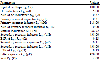
The experimental waveforms of the drive voltage G2 for the IGBT S2 and the resonant voltage vCp across capacitor CP are shown in Fig. 8. From Fig. 8, it can be seen that S2 is turned on when vCp is less than zero,and S2 is turned off when vCp is greater than zero. Similarly, it is easy to be found that switching state is changed when vCp is equal to zero. So, the conclusion that IGBTs S2 and S3 work in zero voltage soft switching state can be easily obtained.
Therefore, on the basis of a comprehensive analysis of the experimental waveforms Fig. 7 and 8, the conclusion that the two primary IGBT switching pairs (S1, S4 and S2, S3) work in zero voltage soft switching state can be clearly obtained.
The experimental waveforms of the drain to source voltage of Q1, Q2, Q3, Q4 and the current iLs2 flowing inductor LS2 are shown in Fig. 9.
 | |
| Fig. 8: | Experimental waveforms of G2 and vCp |
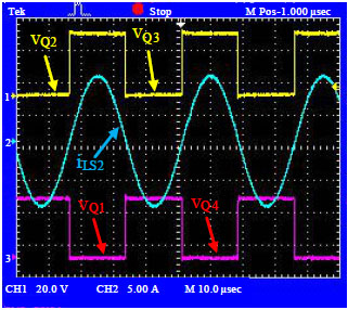 | |
| Fig. 9: | Experimental waveforms of vQ1, vQ2, vQ3, vQ4 and iLs2 |
From Fig. 9, it can be seen that switches Q1, Q4 are simultaneously turned on when vCp is greater than zero,and Q1, Q4 are simultaneously turned off when vCp is less than zero. At same time, it can also be found that the switching states of Q1 and Q4 are changed when the current iLs2 is equal to zero.
Operation of switches Q2 and Q3 can be also obtained by analyzing Fig. 9. From Fig. 9, it can be seen that switches Q2, Q3 are simultaneously turned on when vCp is less than zero and Q1, Q4 are simultaneously turned off when vCp is greater than zero. At same time, it can also be found that the switching states of Q2 and Q3 are changed when the current iLs2 is equal to zero.
Hence, on the basis of a comprehensive analysis of the experimental waveforms (Fig. 9), the conclusion that the two secondary MOSFET switching pairs (Q1, Q4 and Q2, Q3) work in zero current soft switching state can be clearly obtained. This means that the secondary full-bridge SR network works in zero current soft switching state.
Therefore, the experimental results show that zero voltage soft switching state of the primary full-bridge and zero current soft switching state of the secondary full-bridge SR network have been achieved in the IPT resonant converter.
REFERENCES
- Yeh, C.A. and Y.S. Lai, 2012. Digital pulsewidth modulation technique for a synchronous buck DC/DC converter to reduce switching frequency. IEEE Tran. Ind. Electron., 59: 550-561.
CrossRef - Coban, A. and I. Cadirci, 2011. Active clamped two-switch forward converter with a soft switched synchronous rectifier. IET Power Electron., 4: 908-918.
CrossRef - Jeong, G.Y., 2008. High efficiency asymmetrical half-bridge converter using a self-driven synchronous rectifier. IET Power Electron., 1: 62-71.
CrossRef - Kim, K.T., J.M. Kwon, H.M. Lee and B.H. Kwon, 2014. Single-stage high-power factor half-bridge flyback converter with synchronous rectifier. IET Power Electron., 7: 1-10.
CrossRef - Dai, X. and Y. Sun, 2014. An accurate frequency tracking method based on short current detection for inductive power transfer system. IEEE Trans. Ind. Electron., 61: 776-783.
CrossRef - Liu, C., A.P. Hu and N.K. Nair, 2011. Modelling and analysis of a capacitively coupled contactless power transfer system. IET Power Electron., 4: 808-815.
CrossRef - Tang, C.S., Y. Sun, Y.G. Su, S.K. Nguang and A.P. Hu, 2009. Determining multiple Steady-state ZCS operating points of a Switch-mode contactless power transfer system. IEEE Trans. Power Electron., 24: 416-425.
CrossRef - Sun, Y., C. Tang, A.P. Hu, H.L. Li and S.K. Nguang, 2011. Multiple soft-switching operating points-based power flow control of contactless power transfer systems. IET Power Electron., 4: 725-731.
CrossRef