
Fang- Hsi Kuo
Department of Information Management, Jin Wen Institute of Technology, Taiwan, Republic of China
Information Technology Journal
Year: 2006 | Volume: 5 | Issue: 2 | Page No.: 364-372


ABSTRACT
In this study we brought up a design environment of reconfigurable computing system for college education. It includes a suite of software named RePCI Tool and a multi-FPGA PCI board named PCI-mFCU. In order to meet the requirements of more and more functionalities, complexities and shorter and shorter time-to-market of products, the environment also including an Intellectual Property library (IP Library). Hardware designers could reuse IP library to reduce the development time. After that, designers could verify their designs by PCI-mFCU. Using the proposed design environment, our students could learning digital logical design step by step from create basic component to function implement and target to system design by VHDL. Finally, we develop and verify some image processing applications using this rapid prototyping system with RePCI Tool and PCI-mFCU.
PDF Abstract XML References
How to cite this article
Fang- Hsi Kuo, 2006. Prototyping a Reconfigurable Computing System for Education. Information Technology Journal, 5: 364-372.
DOI: 10.3923/itj.2006.364.372
URL: https://scialert.net/abstract/?doi=itj.2006.364.372
DOI: 10.3923/itj.2006.364.372
URL: https://scialert.net/abstract/?doi=itj.2006.364.372
INTRODUCTION
In the trend of product development, the product life cycle is getting shorter, but the functionalities and complexities are getting higher. These factors would block the designers and manufactories designing new products. In other words, the problem is the speed of designer designing new product can not reach the speed of the complexity and functionality that product needed. In this reason, it is a tendency for speed up the product design by using IP.
In the recently system development, most requirements of users are achieved by using pure hardware or pure software. The advantages of pure software system development are easy development, high flexibility, easy to modify, development time and cost lower than hardware need. But the defect of pure software development is the performance not good enough to execute part of operations such as images encode/decode data encryption/decryption. It can be observed easily and be a fatal drawback in the efficiency first times. In the other side, developing system by hardware could get higher performance, while it needs long develop time, no flexibility in designing system, high cost. Therefore, it could solve problems more efficiently by using a reconfigurable computing system[1-5] which is give consideration to hardware and software system development. In this system, hardware part could be modified by software part’s requirements. Hardware circuits could be fast developed configured to share software tasks. This system combined the flexibility of software and the speed of hardware. Furthermore, it could accelerate the time to design customized hardware by integrating an IP library into reconfigurable computing system. Therefore, the cost of system development is lower, the reuse of source code is higher. For these reasons, system development time could be shorter.
In this study, we proposed a design environment named RePCI Tool. Hardware designer could use an IP Library in RePCI. This IP library offers a wizard to select IPs by the user. After selecting the IPs, the wizard will generate a Hardware Description Language[6,7] of IPs component architecture. By using components, it increases the flexibility and hierarchy of design. RePCI Tool also provides functions to edit the design synthesize the design, place and route the design. In the verification, this study also provides a reconfigurable computing hardware called PCI-mFCU. User could use PCI-mFCU by assessing Peripheral Component Interconnect, PCI interface. The PCI-mFCU could share tasks from software to raise the system performance. Finally, in the application part, we design and verify some image processing functions by using this design environment.
BACKGROUND OF RECONFIGURABLE COMPUTING SYSTEM
Before going deep into this study, we will make an introduction as background to Field Programmable Gate Array (FPGA) and reconfigurable computing system.
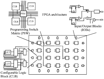
Field Programmable Gate Array (FPGA): FPGA is a hardware which can be reconfigured in seconds. Its main components are Configurable Logic Block (CLB), Input/Output Block (IOB), Programmable Switch Matrix (PSM) and Others. The basic architecture of FPGA is shown in Fig. 1.
 | |
| Fig. 1: | Basic architecture of FPGA |
Because of using Xilinx Spartan-II FPGA[8,9] in this study, we target to Spartan-II FPGA as example.
Configurable Logic Block (CLB):The main and most important component of FPGA is CLB. While Logic Cell (LC) is the basic building block. One LC contains 4-input function generator, carry and Control Logic and Storage element. The input of function generator will drive the input of CLB and the input of D-flop-flop. Each Spartan-II CLB contains four LCs. The function generator is made of lookup table. This lookup table provides 4 bit input data and calculates various functions by using the lookup table. The Carry and Control Logic can provide high speed carry-in operation. Storage element can be configured as edge triggered D Flip-flop or level-sensitive latch.
Programmable Switch Matrix (PSM): The PSM is a matrix which is decided the layout by the commercial tool, ISE, foundation, or Webpack. This matrix can be reconfigured to increase the flexibility of hardware use. While getting the flexibility, it lost the speed. PSM always become the bottleneck of FPGA, because it has the longest delay path. PSM use most area of FPGA above all other components.
Input/Output Block (IOB): IOB is an input/output block which is used of receiving any standard input/output signals outside from the chip.
Others: FPGA contains some other components like Blocked RAM, multiplier, high speed arithmetic logic, Tristate Buffers so on. Those components are different by FPGA series and can be used by HDL.
Re-configurable computing: In the traditional system program design, programmer chooses software or hardware to solve their problems. Using hardware is better or using software. It will explain the advantages and disadvantages of using hardware or software.
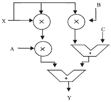
In the aspect of hardware, it executes program by spatial execution, that is to say, hardware costs more area to get the speedup. Hardware is designed sophisticated previous and can execute programs in parallel shown in Fig. 2. Therefore, high speed execution is an important advantage. The disadvantages of hardware are long design time, accept only specific operator and fixed architecture. Cannot to be changed is the main drawback.
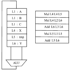
In the aspect of software execution, software use sequential execution to solve program, shown in Fig. 3. Sequential execution needs more time to decode the instruction, move data that the instruction needs. Therefore the execution time is much longer than hardware execution. The advantages of software are short developing time and flexibility.
As is described above, both hardware and software execution has its advantages and disadvantages. In this reason, we would like to design a reconfigurable computing develop environment to combine the high speed of hardware with the flexibility of software.
 | |
| Fig. 2: | Hardware execution |
 | |
| Fig. 3: | Software execution |
Besides, it is necessary to build an IP Library to speed up the design time. By using this IP Library, these IPs could be reuse. The speed up can be obviously observed when execution specific execution such as for and while instructions in software.
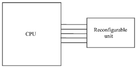
The fastest architecture of all the architecture of reconfigurable computing system[10] is functional unit[2,5] Fig. 4. This functional unit works like cache and put in CPU when designing and manufacturing CPU. The functional unit can be reconfigured as instructions to be called by software. Some reconfigurable computing architecture like Chimaera[1] from Northwestern University can be partial configured. Because of the consideration of cost, the size of functional unit is not large. Therefore, the functional unit always configured as custom instruction. By matching the functional unit, it needs to modify the compiler to use the functional unit.
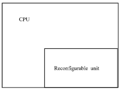
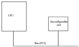
The second kind architecture of reconfigurable computing system is co-processor (Fig. 5). Co-processor is put out of CPU and communicated with CPU by fixed and limited bandwidth. The reconfigurable unit is used as co-processor. For example, in 80486, Intel added a floating point unit outside of CPU. At that time, CPU has two types. One CPU has floating point unit named 486DX. Another has no floating point unit called 486SX. Other architecture researches like OneChip[3] and GARP[4].
 | |
| Fig. 4: | Functional unit |
 | |
| Fig. 5: | Co-processor |
 | |
| Fig. 6: | Standalone processing unit |
In order to lower the uncertain factor, cost and complexity, we forsake the high performance of functional unit to choose the high portability of Standalone Processing Unit[11,12] (Fig. 6). The reconfigurable unit is connected with system bus or external bus. Because accessing the bus, the performance is much lower. The virtues of the architecture are low cost, high portability and needless to modify the compiler to fit the architecture.
Re-configurable computing and its development environment: In this section, we will describe the reconfigurable computing develop environment. The development environment combines two parts, one is RePCI Tool and the other is PCI-mFCU. The design flow is shown in Fig. 7 and each part of the environment is described below. The multiple FPGA partition phase is being develop now, not includes in this study.
RePCI tool: We always make a circuit as component when designing digital circuit by HDL. Components make the management and usage much easily. Components also make the single simulation possible to lower the risk of designing a huge system. We can design system made up of small components. By this reason, we implement a graphical user interface, RePCI shown in Fig. 8, with IP library. RePCI provides some functions: HDL edit, hardware synthesize, hardware place and route and hardware configure.
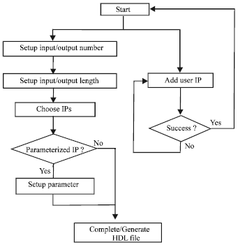
The IP library provides IP functions not only the four fundamental operations of arithmetic but also provides general logic circuits and parameterized IP. User could use the IP Library by a wizard and setup user design step by step. The IP Library design flow is shown in Fig. 9. After setup the design by the wizard provided by IP library, the wizard will generate a HDL file which is composed of HDL components. Finally, user needs to port map the components themselves to complete the hardware design.
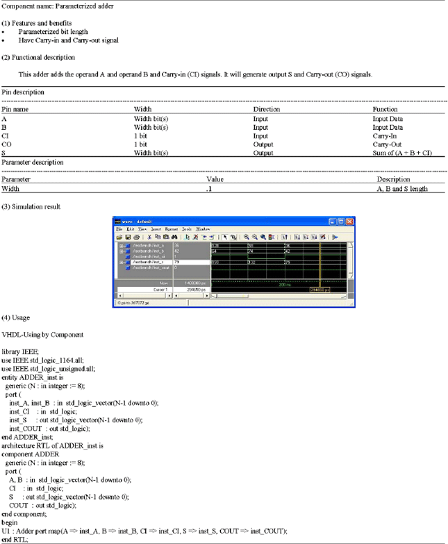
The IP Library contains lots of IP components which are listed in Table 1 those are created by our students. Each IP has its own document with it which is shown in Table 2, Adder for example.
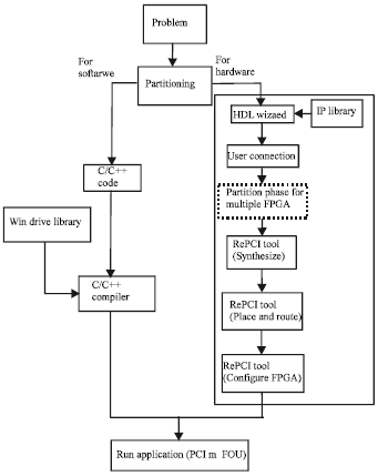 | |
| Fig. 7: | System design flow |
If the input/output length of IP is not big enough, it could combine smaller components to be a big component. Above all, user can also add user created IP into the IP library for further use.
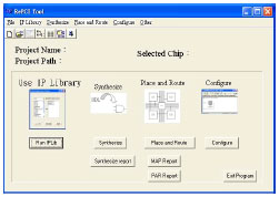 | |
| Fig. 8: | RePCI tool interface |
After port map the HDL file generated by IP library wizard, it can be synthesize, place and route and configure by RePCI Tool. There are two ways to configure FPGA. One way is configure by JTAG port, another way is configure by Peripherals Component Interconnect (PCI) interface.
Using PCI interface to configure FPGA is faster than using Parallel/Serial Port. Not only the advantage of speed up the configuration time, but also add the advantage of another kind of partial configuration. That is to say, in the hardware develop environment, we could configure the second FPGA or the third FPGA even when the first FPGA is still execution.
It is a tragedy that the PCI configuration mode is not support by commercial Electronic Design Automation (EDA) tool. So, we have no choice but to transfer the bitstream file to Serial Vector Format (SVF)[13,14].
| Table 1: | IP List in IP library |
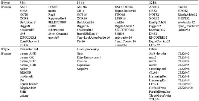 | |
| Table 2: | Parameterized adder document |
 | |
After transferring bitstream file to SVF file format, we must transfer the SVF file to Joint Test Action Group (JTAG) data to configure the devices. JTAG data contains four standard data like Test Mode Select (TMS), Test Data In (TDI), Test Data Out (TDO) and Test Clock (TCK). By using the four signals, we could configure devices by boundary scan mode.
 | |
| Fig. 9: | IP library design flow |
Therefore, when choosing to use the PCI mode, it is necessary transferring the bitstream to SVF.
PCI-mFCU: The PCI-mFCU architecture is shown in Fig. 10. The PCI-mFCU architecture is implemented by the architecture of standalone processing unit mentioned interface. The other motivation is that we could configure FPGA using PCI interface. Because of large size FPGA is still very expensive; we can use multi-fpga to solve this problem. PCI-mFCU is a board with multi-fpga on it. We can partition the big design into two or three designs in order to realize the big design in low cost platform. There are some main components in our hardware platform:
| • | PCI controller: PLX9052[15] Peripheral Component Interconnect. |
| • | Four Xilinx FPGA: Three XC2S100 TQ-144 and one XC2S100 PQ208. |
| • | Electrically Erasable Programmable Read-Only Memory (EEPROM) : XC18V01 |
| • | Oscillator Crystal (OSC) |
PLX9052 is a commercial PCI controller. By using PLX9052, we can access PCI bus without knowing the PCI protocol. PXL9052 is a high speed bus slave interface. It can be a bridge between local bus and slow local bus. The performance of PLX could reach to 132MB/s in the burst mode.
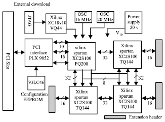 | |
| Fig. 10: | PCI-mFCU architecture |
We could use driver and PLX9052 to access our FPGA.
The function of FPGA is to implement user design. It handles real control and calculation in the design. There are physical connections between FPGA and FPGA. By using these connections, FPGA can communicate with neighbor FPGA.
XC18V01 take the role of load the design to FPGA while the power is on. The oscillator handles trigger the PCI controller and FPGA.
Above all, we can use RePCI Tool to design, synthesize, place and route hardware design and configure hardware design into FPGA. Finally, we can verify the hardware design by using PCI-mFCU development board.
APPLICATIONS AND RESULTS
After making an introduction to our development environment, we will develop some image processing functions by using the RePCI Tool and PCI-mFCU. Image processing applications always execute the same operations; it is suitable to accelerate by hardware. And the image processing applications ranging from medical science to industrial image recognize, that means it is wide area knowledge. We have developed four filter-functions (IP) for image processing applications. All these functions are operating with the nine-cell window (Fig. 11) pixel by pixel until all pixels of the image are calculated. After that, we can design C program accessing PCI to use the image processing hardware.
Before designing the image processing application, we have to know the content of image. We will describe the bitmap format below.
| Fig. 11: | Nine-cell window |
 | |
| Fig. 12: | BMP file format |
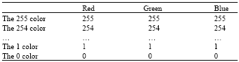
The format of Bitmap contains three part, File Header, Palette and Image Data. The data of file header contains the characteristic of image, such as the width of image, size and colors and so on.
Palette contains all of the colors that image can be use. Image Data records the red, green, blue value of each pixel. For example, an image has 16 pixels in its width and height and there are 256 colors in each pixel color. The width, height, 256 colors need to be stored in file header. Palette will store the colors that each pixel used, shown in Fig. 12.
Therefore, we can imagine the palette as a table. Each pixel has three colors, red, green blue. The content of the table is the weight of color brightness. Gray palette is used most frequently. All colors in the palette are gray. There is no different color in gray palette but brightness.
Next data of the format is image data. The data contains the value of each pixel. Bitmap image format always use 24 bit color to storage the red, green, blue colors. All of the three colors have eight bits width to storage the weight. The maximum data of eight bits can reach 256 data. Therefore each color’s value should range from zero to 255. For instance, the value of pixel is zero means this pixel is black. The value of pixel is 255 means white. The value of pixel is 128 means gray.
Image processing applications always get the values of RGB in the original picture and doing some specific process. For example, if we want to transfer 24 bits full color to gray color, we need to get the RGB color and doing some specific calculation then save to another picture. It will be continued until all the pixels are completely calculated.
Function one: Edge enhancement: Here we will use RePCI tool to develop the application of edge enhancement. The principles of edge enhancement are described below. First, we need to get the eight data (p [1] ~p [4] and p [6] ~p [9]) around the determined pixel (p [5]). Secondly, we could calculate by the following equation: (p[7]+(p[8]*2)+p[9])-(p[1]+(p[2]*2)+p[3]). Third, we must saving the calculated data to a new image.
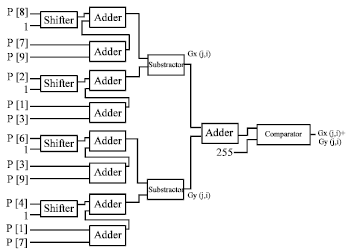 | |
| Fig. 13: | Edge enhancement hardware chart |
 | |
| Fig. 14: | Image expansion hardware chart |
 | |
| Fig. 15: | Image erosion hardware chart |
 | |
| Fig. 16: | Negative hardware chart |
The edge enhancement could be completed when all pixels are done by the three steps. When the processing algorithms are different, the result of image will different through.
When designing the hardware, it needs to put the data (p [1] ~p [4] and p [6] ~p [9]) in the inputs. Then get the data from the output, (Gx (j, i) + Gy (j, i)). In other words, if we send data to the hardware, it will calculate the result for us. It is much faster than software execution, because it needless to decode instruction, fetch instructions and so forth.
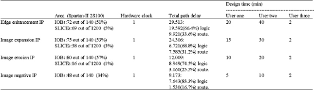
| Table 3: | Image Processing synthesized result and design time table |
 | |
In the application, we need a shifter, adder, substractor and comparator to complete the design. The full hardware design chart is shown in Fig. 13.
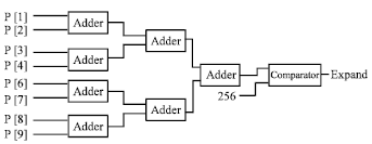
Function two: Image expand: The theorem is much similar between edge enhancement and image expansion. It needs to get the data (p[1]~p[4] and p[6]~p[9]) to be calculate by the following equations: (p[1]+p[2]+p[3]+p[4]+p[5]+ p[6]+p[7]+p[8]+p[9]). After calculation, we must check the correct return value for new picture. In order to design the image expansion application, we need eight bit adder, nine bit adder and ten bit adder, the hardware design chart is shown in Fig. 14.
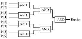
Function three: Image erosion: The theorem of designing the image erosion is much similar with image expansion. It needs to get the data (p[1]~p[4] and p[6]~p[9]) to be calculate by the following equations:
(p[1]&p[2]&p[3]&p[4]&p[5]&p[6]&p[7]&p[8]&p[9]). |
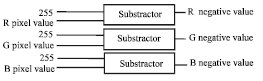
Function four: Image negative: The theorem of image negative is to subtract each pixel from 0xFF and we will get the new pixel value. In order to design the hardware of image negative, we need eight bit subtractor. The hardware chart is shown in Fig. 16.
Finally, the synthesized results of all applications are shown in table three. Because of the powerful of the EDA tool and FPGA, the FPGA resource that applications used is not much. Because the execution speed of FPGA is quick enough, software can get the final execution result from hardware immediately. The column of design time in the Table 3 lists the design time of three designers designing the same hardware including the simulation time. User one selected from our senior students is familiar with the EDA tool and the basic HDL concept. User two selected from our junior students is not familiar with the HDL and EDA tool. User three is one student of our lab. They are designing the same hardware which is mentioned above. User one and user two designing the hardware with no RePCI tool and user three designing the hardware with RePCI tool As is known in table three, it can get lower time to design the same hardware by using RePCI tool.
In order to emphasize the importance of system performance, while implement the image processing application using above functions, we divide the original image quarterly, since the PCI-mFCU have four FPGA on it. The image data of each quarter are rippled by nine-cell window scan method individually.
CONCLUSIONS
In this study, we proposed the education purpose design environment (RePCI Tool and PCI-mFCU) for developing reconfigurable computing system. In the software part, user could setup their hardware design by using IP Library in RePCI Tool. After completing the hardware designs, user could synthesize, place and route and configure the designs by using RePCI Tool. In the hardware part, user could verify their hardware design by using PCI-mFCU. PCI-mFCU allows user communicating with it by accessing the PCI interface. PCI-mFCU is a multi-FPGA board, it makes large design could be realized in low cost environment. Finally, we implement some image processing applications to verify the whole system.
FUTURE WORK
Our design environment is not very perfect by obverting from the application results. First, the architecture of the PCI-mFCU takes much time in accessing PCI bus. In order to decrease the slow data arriving time, we should change the architecture from standalone processing unit to functional unit. Secondly, it is necessary to having more graphical user interface provided by RePCI. It can make the usage more easily. Third, it needs to have more functional complete hardware designs such as Filter, CPU, Universal Asynchronous Receiver/Transmitter (UART) to fit the further design use.
REFERENCES
- Hauck, S., T.W. Fry, M.M. Hosler and J.P. Kao, 2004. The chimaera reconfigurable functional unit. IEEE Trans. Very Large Scale Integr. Syst., 12: 206-217.
CrossRefDirect Link - Razdan, R. and M.D. Smith, 1994. A high-performance microarchitecture with hardware-programmable functional units. Proceedings of the 27th Annual International Symposium on Microarchitecture, San Jose, California, USA., Nov. 30-Dec. 02, ACM, New York, USA., pp: 172-180.
CrossRefDirect Link - Wittig, R.D. and P. Chow, 1996. One chip: An FPGA processor with reconfigurable logic. Proceedings of IEEE Symposium on FPGAs for Custom Computing Machines, April 17-19, Napa Valley, CA, USA., pp: 126-135.
CrossRefDirect Link - Hauser, J.R. and J. Wawrzynek, 1997. GARP: A MIPS processor with a reconfigurable coprocessor. Proceedings of IEEE Workshop on FPGAs for Custom Computing Machines (FCCM), April 16-18, Napa, CA, pp: 12-21.
CrossRefDirect Link - Brown, S. and J. Rose, 1996. FPGA and CPLD architectures: A tutorial. IEEE Design Test Comput., 13: 42-57.
CrossRefDirect Link - Compton, K. and S. Hauck, 2002. Reconfigurable computing: A survey of systems and software. ACM Comput. Surveys, 34: 171-210.
CrossRefDirect Link