
Shi-Hai Zhu
Department of Computer and Information Engineering, Zhejiang Water Conservancy and Hydropower College, China
Information Technology Journal
Year: 2013 | Volume: 12 | Issue: 5 | Page No.: 943-950


ABSTRACT
Hardware interrupt management method based on field programmable gate array is proposed in this study according to the requirement of embedded real-time operating system for real-time performance and the structure model of interrupt management module is also given. Interrupt is subdivided into system and user interrupts owing to different characteristics of interrupt request and response method. Interrupt source management, interrupt vector management, interrupt nesting and clock tick interrupt management have all been implemented by hardware. The simulation results show the feasibility and stability of this kind of interrupt management method. In a word, the implementation of interrupt management by hardware improves not only the utilization rate of CPU, but also the real-time performance of the whole system.
PDF Abstract XML References Citation
Received: September 02, 2012;
Accepted: December 17, 2012;
Published: February 18, 2013
How to cite this article
Shi-Hai Zhu, 2013. Hardware Implementation Based on FPGA of Interrupt Management in a Real-time Operating System. Information Technology Journal, 12: 943-950.
DOI: 10.3923/itj.2013.943.950
URL: https://scialert.net/abstract/?doi=itj.2013.943.950
DOI: 10.3923/itj.2013.943.950
URL: https://scialert.net/abstract/?doi=itj.2013.943.950
INTRODUCTION
Embedded Real-Time Operating System (ERTOS) is widely used in strong real time systems, for example, a new generation of fighters, aerospace system and so on. People have a higher requirement on its real-time performance because it has been applied to more and more extensive fields. With the continuous improvement of integration level of Field Programmable Gate Array (FPGA) and its speed, it is possible to implement ERTOS by hardware (Mooney and Blough, 2002; Xia, 2010).
Interrupt is a kind of hardware mechanism and can be divided into two parts: interrupt controller and interrupt management. Interrupt controller is responsible for receiving interrupt, judging interrupt source and recognizing interrupt. Once interrupt has been identified, interrupt controller saves field data to stack space manager and the corresponding Interrupt Service Routine (ISR) is executed. After that the program returns to the breakpoint and continues executing the next instruction. By contrast, interrupt management part belongs to the upper module, which is different from the kernel management of Operating System (OS). As is known to all, different OS has its specific interrupt management method (Jianhua et al., 2008; Cho et al., 2005; Mooney, 2003).
In VxWorks operating system, interrupt management is performed by connecting the specific pins of CPU to different peripherals and setting low level voltage to generate different interrupt signals. Among them, each interrupt pin of CPU corresponds to an interrupt number and it is bound together with its ISR. When interrupt occurs, its corresponding ISR is automatically called. Thus each time when the data of hardware are ready, CPU can timely get them in this way (Jing and Zhi-Wei, 2004). In Linux kernel, interrupt handler is divided into two kinds: slow speed and fast speed (Qiuping, 2007). Usually Linux kernel divides interrupt handler into two parts: the upper half and the lower half. Generally speaking, the latter part is time-consuming (Xuesong et al., 2007). When an interrupt occurs, the upper part of interrupt handler is performed, it stores the data to be dealt with to the specified equipment buffer, marks the lower part and then exits (Feng et al., 2001; Yufeng and Baohua, 2008).
In μC/OS-II operating system, interrupt is realized by calling the interrupt service routine written by the assembly language. When an interrupt occurs, some registers of CPU are automatically pushed into the stack and interrupt nesting is allowed so long as the interrupt service routine is written to enable next interrupt. The unique communication method between a task and interrupt service routine is used through global variables. At the same time, μC/OS-II also provides periodical signal source, namely, clock ticks to implement time delay and confirm timeout (Jijun, 2008). Clock tick source can be either special hardware timer or 50/60 Hz AC power signal. It is notable that clock metronome is opened after the multitasking system is started (Xiaogang and Yimin, 2007). In this study an interrupt management method based on PowerPC architecture is proposed and implemented by FPGA hardware.
DESIGN OF INTERRUPT MANAGEMENT
The overall framework of interrupt management: First of all, interrupt is divided into two kinds: system and user interrupt. System interrupt handles the interrupt caused by the system, while user interrupt handles external interrupts available for the users. Interrupt trigger signal is set by separate I/O pins of FPGA, each pin corresponds to one external interrupt or multiple external interrupts correspond to one interrupt handling task.
As shown in Fig. 1, interrupt system is in charge of notifying all external interrupts except system interrupt and it can also send interrupt enable signal to the hard kernel to find interrupt source. In the hard kernel, interrupt service routine is called interrupt task, which is scheduled by the hard kernel like ordinary tasks. When external interrupt comes, the scheduling mechanism of hard kernel is triggered and interrupt task is executed just-in-time.
Interrupt handling process
System interrupt: In PowerPC architecture, all interrupts except external interrupt and maskable external interrupt are called system interrupts. For example, system runaway in Xilinx Virtex-II Pro hardware platform belongs to system interrupt. When system interrupt occurs, there exists a unified system interrupt service routine entry, only a small amount of necessary register data need to be stored before execution. The workflow of system interrupt handling is described below:
| Step 1: | When an interrupt occurs, hardware finds unified system interrupt entry address from interrupt vector module and interrupt task starts executing from this entry |
| Step 2: | It saves the values of some CPU registers |
| Step 3: | At the same time, it can get interrupt number from interrupt source management module and interrupt vector address from interrupt vector management module |
| Step 4: | It executes corresponding interrupt service routine according to interrupt vector entry address |
| Step 5: | After the execution of interrupt service routine, it restores the saved register values |
| Step 6: | It returns from interrupt, the program continues to execute from the breakpoint |
User interrupt: External interrupt and maskable external interrupt are called user interrupts (Cheng-Min, 2010). External interrupt is triggered by FPGA pin, while maskable external interrupt is triggered by other modules on chip. The workflow of user interrupt handling is described as:
| Step 1: | When an interrupt occurs, hardware finds unified user interrupt entry address according to interrupt vector register and interrupt task starts to execute the following interrupt operations from this entry |
| Step 2: | It saves the values of registers in interrupt controller and CPU, writes them to the corresponding stack space manager, at the same time masks those lower priority interrupts than this interrupt |
| Step 3: | It enables new interrupt, gets interrupt source and finds the entry address from the interrupt vector module in order to execute corresponding interrupt service routine |
| Step 4: | It finishes interrupt handling and performs stack pointer switching. First of all, it judges where to exit from the interrupt, if the task is exited from interrupt, then it needs to switch from interrupt nesting stack to task stack, otherwise if the task is exited from the nested stack, then it needs no stack switching |
| Step 5: | It restores the saved register values in step 2 |
| Step 6: | It exits from interrupt and continues to execute the interrupted program |
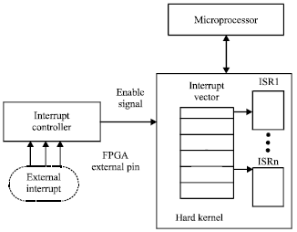 | |
| Fig. 1: | The overall framework of interrupt management |
THE INTERNAL STRUCTURE OF INTERRUPT MANAGEMENT MODULE
As shown in Fig. 2, interrupt management module consists of the following four parts: interrupt source management logic, interrupt vector management logic, interrupt nesting logic and clock tick interrupt management logic. Among them, interrupt source management logic generates the Id (identifier) of interrupt source; interrupt vector management logic provides unified entry address; interrupt nesting logic judges whether there exists interrupt nesting among user interrupts, if so then it needs no switching interrupt nesting stack, otherwise it needs switching to task stack to continue executing; clock tick interrupt management logic belongs to system interrupt and it contains a clock counter register.
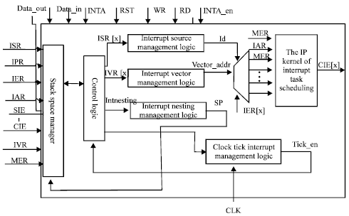 | |
| Fig. 2: | The internal structure of interrupt management module |
 | |
| Fig. 3: | The specific workflow of interrupt management |
As soon as the clock tick arrives, it executes interrupt task.
It can also be seen that hardware interrupt management is quite different from interrupt controller. If interrupt enable signal of interrupt controller is effective, INTA_en equals 1 and external interrupt arrives then interrupt handling is executed. At the moment the operating system's hardware interrupt task scheduler performs the unified scheduling and completes interrupt task management. Most of the operations don't need CPU’s participation, thus saving the overhead of CPU.
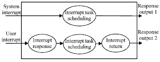
In this interrupt management module, system and user interrupt can both be realized. The difference between interrupt management module and traditional interrupt controller is that interrupt request is directly proposed to the operating system but not CPU. When external interrupt arrives, interrupt task is set to ready state and is uniformly scheduled by hardware task scheduler of the real-time operating system. Interrupt management module just receives interrupt request, sets the corresponding interrupt task to ready state and during this process it does not need CPU interrupt response cycle as in traditional interrupt controller. The specific workflow is shown in Fig. 3.
HARDWARE IMPLEMENTATION OF INTERRUPT MANAGEMENT MODULE
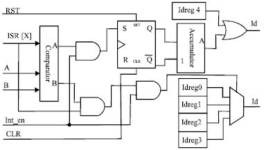
Interrupt source management logic: Five kinds of interrupt sources are defined in interrupt management, they are listed below: external equipment request interrupt, fault forced interrupt, clock tick request interrupt, data channel interrupt and program self-trapping interrupt. Among them, external equipment request interrupt is defined as user interrupt and all the other interrupts are defined as system interrupts. System interrupt can directly perform task scheduling, whereas user interrupt requires all the procedures of interrupt response, task scheduling and interrupt field recovery. Each FPGA pin corresponds to a kind of interrupt, a kind of interrupt may have different interrupt types, so this design can meaningfully save hardware resources to some extent. The main task of interrupt source management logic is to receive interrupt enable signal and identify the interrupt sources. If the same kind of interrupt source applies for an interrupt, then trigger signal is created, a suitable interrupt source Id is allocated; but if not, then interrupt source Id is directly distributed, as shown in Fig. 4.
As mentioned above, five kinds of interrupt sources are respectively described as ISR0, ISR1, ISR2, ISR3 and ISR4. Among them, ISR0~ISR3 correspond to system interrupts; namely, they are defined as B signals.
 | |
| Fig. 4: | The logical circuit diagram of interrupt source management |
| Table 1: | Interrupt type number register |
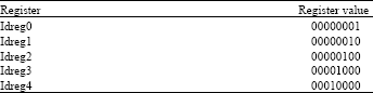 | |
By contrast, ISR4 stands for user interrupt, namely, defined as A signal. The type number of interrupt source is defined by Idreg0~Idreg4 registers, as shown in Table 1.
The interrupt type number relates to interrupt task priority, the smaller the interrupt type number, the higher the interrupt task priority. The workflow of interrupt source management logic is described in detail below: First, it judges interrupt source is system or user interrupt, if output signal A is effective, then interrupt source is user interrupt; if output signal B is effective, then interrupt source is system interrupt. Second, for user interrupt if the interrupt enable signal given by interrupt controller is effective, then it is sent to a trigger to generate a trigger signal, that is received by the accumulator which performs the operation of adding 1. Next Idreg4 and the accumulator performs or operation to generate a new Id and output it. In this case user interrupt can support the maximum number of 15 external interrupts. Finally, for system interrupt the selector must make a choice from interrupt type number register and directly output interrupt type number Id.
Interrupt vector management logic: Its main task is to receive the value of interrupt vector register (IVR[x]) in the interrupt controller and to construct an interrupt vector register group to save interrupt vector values. Then it selects interrupt vector address through the selector and points to a particular entry address of interrupt service routine. Besides, it establishes an interrupt vector register group called IVRreg and the interrupt vector values of ISR0~3 which correspond to system interrupt vectors are separately stored in them.
 | |
| Fig. 5: | Interrupt nesting schematic diagram |
By contrast, user interrupt vector address starts from IVRreg4. When user interrupt occurs, interrupt vector is saved in turn to this interrupt vector register, but the number of user interrupt can not exceed 15.
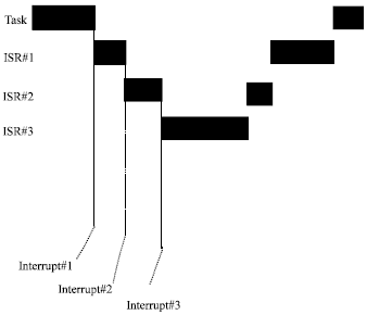
Interrupt nesting logic: Interrupt nesting refers to that interrupt system can identify another more important interrupt and serve for it during an interrupt service, as shown in Fig. 5.
Interrupt nesting logic judges whether there exists interrupt nesting through the IntNesting field, if the value of IntNesting equals 0 then it means that there does not exist interrupt nesting, this interrupt directly returns to the breakpoint and SP pointer jumps from interrupt nesting stack to task stack. Otherwise if not so then it means that there does exist interrupt nesting, SP pointer reads interrupt task information saved in interrupt nesting stack and responds nested interrupt before this interrupt is completed. SP pointer does not jump from interrupt nesting stack to task stack until IntNesting is 0.
Clock tick management logic: The solution to hardening clock tick management is listed below:
| Step 1: | It receives clock tick interrupt source and stores such information as delay time, task ID, task priority in the input register TTDelayreg |
| Step 2: | The timer produces clock ticks. It scans TTDelayreg register at each clock tick to judge whether there is a task whose delay time is already full. If so then interrupt request signal of clock tick is set to 1, it sets highest priority task to ready state, waiting for executing. If not so then delay time field of the task is subtracted a clock tick. Steps (1) and (2) are repeatedly executed until all the tasks are over. If the value of this register is empty then clock tick management logic is set to dormant state until new clock tick interrupt task comes |
| Step 3: | If clock tick management logic receives the signal to recover task delay, then interrupt request signal of clock tick is set to 1, the task delay is canceled and the task is set to ready state |
SIMULATION RESULTS ANALYSIS OF INTERRUPT MANAGEMENT
The timing simulation waveform diagram of interrupt source management is shown as Fig. 6. It can be seen that five kinds of interrupt sources are defined in the interrupt source management module, each interrupt source corresponds to the relevant bit in ISR register. That is, when the interrupt source ISR0 is effective, the value of Idreg0 register equals 00000001; similarly, when the interrupt source ISR1 is effective, the value of Idreg1 register equals 00000010; when the interrupt source ISR2 is effective, the value of Idreg2 register equals 00000100, the detailed information about corresponding registers is shown as Table 1. The simulation diagram adopts decimal notation. Under the condition of interrupt enable signal is effective, if ISR0 is effective, then output Id number is 1; similarly, if ISR1 is effective, then output Id number is 2; if ISR2 is effective, then output Id number is 4; if ISR3 is effective, then output Id number is 8. But ISR4 is different from them, it corresponds to user interrupt, whose Id number is distributed through a trigger mechanism. It can respond three user interrupts, output Id is separately set 16 to 18. The experimental results show that the same user interrupt can get different Id numbers, which illustrates the correctness and feasibility of our design. One interrupt source corresponding to different interrupt types means that external interfaces can be saved.
The timing simulation waveform diagram of clock tick management logic is shown as Fig. 7, the delay management of four tasks is simulated. First, output register group DelayReg is initialized to receive priority, ID, delay_time of the task that needs to delay.
The received data are stored in the input register group TTDelayreg which is not drawn in the simulation diagram. Next the timer is started. Second, it scans the control signals of cancel and time_en. That clock cycle is set to 5 clocks means that every five clocks produce a clock tick and all delay tasks are scanned once.
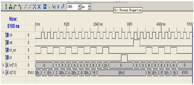 | |
| Fig. 6: | Timing simulation waveform diagram of interrupt source management |
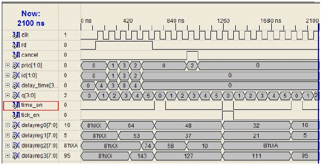 | |
| Fig. 7: | Timing simulation waveform diagram of clock tick management |
If the scanned task meets the expiry of the prescribed period of time or a task calls the cancel control signal then task scheduling is triggered with the result that tick_en is set 1, interrupt task scheduling is performed, otherwise the time of delay task minus 1. It can also be seen that the initial value of DelayReg1 equals 53, namely 00110101 B (binary), after a clock tick the value of DelayReg2 equals 37, namely 00100101 B and the time of delay task minus 1 for the task whose priority is 1.
The simulation results also show that CPU processes delay task and executes task scheduling only after it receives tick_en signal. CPU no longer needs to constantly scan clock tick interrupt service routine so as to increase CPU efficiency and improve system performance.
DISCUSSION
Literature invented the interrupt management method of embedded operating systems based on PowerPC architecture, which improves interrupt execution efficiency more greatly and controls the interrupt more conveniently. But in order to prevent the stack overflow exception caused by nested interrupts, it is necessary to calculate the size of stack space for many times.
Literature invented the interrupt realization method of embedded operating systems based on components, making it is more reliable to realize interrupt; But the operating system needs to supply the services of applying for, receiving, checking and loading the components, therefore the system overhead is bigger.
In the symmetric multiprocessor systems, interrupt controller often uses Advanced Programmable Interrupt Controller (APIC). He mainly introduced the internal structure and working principle of APIC which is widely used based on x86 framework (Xingjie, 2008). But we all know that x86 framework is different from PowerPC framework.
Hierarchical design is adopted to improve the system's portability and guarantee the high efficiency and high reliability of the system according to the disadvantages of traditional interrupt management design (Pu et al., 2003), but there are some deficiencies in the system. First, the interface definition of board level support is not perfect, reducing the system’s portability; secondly, there are not enough custom interfaces for developers in the current data structures, decreasing the scalability of the system.
The model of “former and latter segment interrupt processing” is proposed in embedded kernel interrupt management. In view of the problem of many interrupts share one vector, the processing technology of single vector corresponds to many interrupts is introduced and realized, aiming to improve the real-time performance of embedded real-time system (Hongwei et al., 2004). But it has certain applicable scope of Delta OS and PowerPC MPC860 platform.
An interrupt management model based on integrated priority space was proposed in this study with the result of better performance than the traditional model in certain circumstance (Guo and Zhang, 2007). But it is inconvenient to judge the application scope of this model owing to the complicated computing formula.
The general interrupt handling mechanism of embedded system was first introduced and then the realization of a Linux embedded system interrupt handling mechanism was described in detail by registering a processing procedure for each equipment and programming good interrupt handler, thus processing correctly when an interrupt arrives (Zishi, 2009).
Linux kernel offers the capability of opening and closing interrupt response, but it is difficult to write complete, practical interrupt handler by researching the process management of the kernel deeply.
He analyzes the ARM7TDMI processor vector IRQ interrupt handling process in vision4 development environment, designs a reentrant interrupt system and gives the program code to be realized. The adopted strategy has practical value for real-time embedded systems (Jinping, 2012). The involved program source code was debugged on Vision4 development environment and the generated executable file was tested on Proteus simulation software platform and LPC2138 development board. Therefore, it means little significance for other types of simulation software and development board.
CONCLUSIONS
ERTOS has such advantages as strong real-time performance, high reliability, convenient portability, good safety performance and the like, so it has wide application prospects. This study fully understand the situation of RTOS and interrupt management at home and abroad, designs hardware interrupt management based on FPGA, taking μC/OS-II kernel as an example. It also gives the overall design framework of hardware ERTOS interrupt management. Besides, interrupt is subdivided into system and user interrupt. Task scheduling can be directly performed for system interrupt, but it requires the whole process of interrupt response, task scheduling and interrupt return for user interrupt. The simulation results verify the feasibility of the design and the improvement of CPU’s utilization rate.
In addition, the following two aspects are worth further studying:
| • | Call interfaces are to be perfected. Currently call interface research and design are not involved with the result that this method has not shown very strong practical application value. Therefore, call interface is our main research direction in the future |
| • | Design thought of interrupt management module is to be optimized. Its generality can be expanded and transplanted to more system architectures besides PowerPC |
ACKNOWLEDGMENT
This study was supported by the research foundation of national natural science fund project of China (No. 60972127), under which the present work was made possible.
ABBREVIATIONS
| ISR | = | Interrupt status register |
| IPR | = | Interrupt pending register |
| IER | = | Interrupt enable register |
| IAR | = | Interrupt acknowledge register |
| SIE | = | Set interrupt enables |
| CIE | = | Clear interrupt enables |
| IVR | = | Interrupt vector register |
| MER | = | Master enable register |
REFERENCES
- Mooney, V.J. and D.M. Blough, 2002. A hardware-software real-time operating system framework for SOCs?. IEEE Des. Test Comput. Mag., 19: 44-51.
CrossRef - Cui, J.H., H.S. Sun and B.J. Wang, 2008. The design and realization of hardware real-time operating system. Appl. Electron. Tech., 5: 34-37.
Direct Link - Cheng-Min, L., 2010. Nested interrupt analysis of low cost and high performance embedded systems using GSPN framework. IEICE Trans. Inform. Syst., E93-D: 2509-2519.
Direct Link - Pu, H., H. Liu and M. Ling, 2003. Implementation of interrupt manager in small-scaled embedded operating system. Chin. J. Electron Devices, 26: 218-221.
Direct Link - Guo, J.H. and M. Zhang, 2007. An interrupt management model for real-time system based on integrated priority space. J. Jiaying Univ., 25: 73-76.
Direct Link